Microsoft Reveals Technical Details on Xbox One APU
It's a massive chip, measuring 363 square millimeters.
This week during the Hot Chips engineering conference at the Stanford Memorial Auditorium, Microsoft chip architect John Sell introduced the world to the secretive APU the company jointly developed with AMD. As it turns out, the APU is rather enormous, featuring a 363 square millimeter surface manufactured with TSMC's 28 nm HPM process technology. As a comparison, Intel's 22 nm Core i7-4770K "Haswell" chip measures 177 square millimeters.
Naturally the larger the chip becomes, the more prone it is to forming small defects on the wafer surface that could result in a repeat of the Xbox 360 "Red Ring of Death" fiasco. To generate better yields for the Xbox One generation, Microsoft reportedly designed redundancies into the chip so that if one portion becomes inoperable, the whole chip isn't totally worthless.
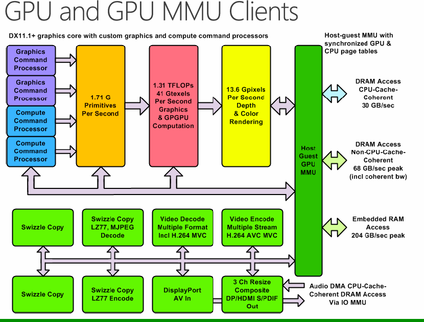
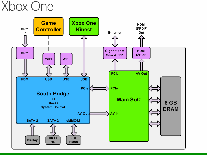
Sell also revealed that the chip packs 5 billion transistors that combines the CPU cores, the GPU core, 47 MB of cache and 32 MB of extra on-chip storage. He said the cache/storage aspect uses up about half of the chip's transistors, and because storage is embedded into the APU, the chip saves power because it doesn't need to constantly access the console's 8 GB of DDR 3 RAM or the 500 GB hard drive.
Article continues belowSell didn't disclose just how much this chip will consume, but said that it will be power gated down to 2.5 percent. The company actually designed small islands and gates within the APU that switches off specific areas so the chip can consume less power when needed.
As previously reported, the APU has eight AMD Jaguar 64-bit CPU cores with 32 KB of instruction and data cache. Four cores will be connected to 2 MB of shared Level 2 cache along with the embedded a graphics DirectX 11.1+ core. AMD revealed this hUMA technology back in April, or rather its Heterogeneous Uniform Memory Access tech that builds upon the Heterogeneous Systems Architecture (HSA).
Essentially shared memory makes life easier for developers and provides overall improved system performance. AMD's Kaveri APUs were the first to take advantage of this tech, and the PlayStation 4 naturally also makes use of this technology given its based on an AMD APU as well.
Getting back to the Xbox One's chip, the GPU portion of the APU will reportedly be accompanied by 15 special purpose processors including four command processors (two compute, two graphics), and two dedicated vector cores for the audio subsystem. The data highways can transfer bits up to 204 GB/s across different parts of the chip, and up to 68 GB/s to the off-chip DDR3 memory.
Get Tom's Hardware's best news and in-depth reviews, straight to your inbox.
In addition to the Xbox One's APU, Microsoft system designer Patrick O’Connor took the stage to talk about the new Kinect's processor and light sensor. The team wanted the sensor to have enough intelligence to distinguish the player from objects in the surrounding area including the couch, the lamp and so on. Thus the device can pinpoint each player less than 3.3 feet away and more than 6.6 feet away using a 70 degree field of view.
O'Connor explained that Kinect "illuminates" the room with its own modulated light, and uses the 512 x 424 sensor to see that reflected light, which will be out of phase depending on how that light is reflected off objects. The console then processes the info to weed out ambient light and to define the actual "active" image. O'Connor said that Kinect supports up to six simultaneous players, but determining who is actually playing takes some processing power.

Kevin Parrish has over a decade of experience as a writer, editor, and product tester. His work focused on computer hardware, networking equipment, smartphones, tablets, gaming consoles, and other internet-connected devices. His work has appeared in Tom's Hardware, Tom's Guide, Maximum PC, Digital Trends, Android Authority, How-To Geek, Lifewire, and others.
-
house70 They need to cool down that thing properly this time. A lot of RROD instances have happened because of chronic overheating leading to premature failure, and people that bit the bullet and applied custom aftermarket cooling hardly had a RROD.Reply -
getochkn Wafer surface has nothing to do with the Red Ring of Death. It's lead-free solder. Same reason PS3's get the Yellow Light of Death, laptop GPU's die and give black screens and a lot of modern day electronics crap out. Lead-free solder isn't as strong, BGA connections either break or form tin whiskers. Companies need to use better solder as there are better lead-free alternatives out there, but it comes down to cost. An extra 40 cents per board to use a better solder or save 40 cents per console/laptop/whatever, they choose to save the 40 cents.Reply -
mobrocket Have people noticed that there is more Xbox One news regarding hardware then PS4...Reply
is that cus MSFT is releasing more, or cus we are in the US... and its the opposite going on in japan? -
Murissokah "Thus the device can pinpoint each player less than 3.3 feet away and more than 6.6 feet away using a 70 degree field of view."Reply
Does that mean it has a blind spot between 3.3 and 6.6? I'm guessing either I didn't understand it or the author slipped there.
Anyway, nice to have some info on the VGA. It is a new architecture with a few significant innovations, so I find it hard to know what to expect before we see it in action.
As for kinect... still don't care about it. It is a shame to see how much time and resources are invested in that. -
the1kingbob Wouldn't it make more sense to compare this APU with a AMD APU? This would help communicate the 'modified' AMD APU they are using. I don't understand why it should be compared with an i7... what does this communicate?Reply -
Bill Reinhardt I'm hoping that the Xbox One and PS4 are too similar to determine a clear winner in the graphics department. Hopefully, it will create better games and exclusives for either system.Reply -
the1kingbob Also, the RROD death wasn't caused by the die size. As mentioned it was caused by lead-free solder. Also, the crappy clips used to hold down the heatsink begin to give way after so many heating/cooling cycles allowing the heatsink to lift off. Most chips, no matter the size, would likely not be able to survive in that situation.Reply -
stevejnb Reply11445372 said:I can't wait to get my hands on a day one Xbox One.
Really? Not only do initial releases of major electronics devices often have hardware bugs to work out in general, after the 360's earlier models obvious flaws, MS should be under extra scrutiny with their first few batches of XBOX One's. Granted, the original XBOX had hardware as solid as a Nintendo device and moreso than any Sony console ever released, but the 360 was an obvious case of shoddy design that took years before it became a piece of hardware without a looming expiration date.
I really quite enjoy my 360, and bought my first one within 6 months of launch, but I'll probably give the XBOX One at least 1 year to work out bugs, build up a game library, and build a bit of good will after the early 360 fiasco. Besides, I've got a huge backlog of 360 and PS3 games to get through - let other people do the beta testing on the new hardware from two companies which have spotty track records for reliable hardware. -
peterson99 Reply11445578 said:Also, the RROD death wasn't caused by the die size. As mentioned it was caused by lead-free solder. Also, the crappy clips used to hold down the heatsink begin to give way after so many heating/cooling cycles allowing the heatsink to lift off. Most chips, no matter the size, would likely not be able to survive in that situation.
Actually, if you've damaged the die (as mentioned in the article) you would get the same ring of death as the overheating. So I think people are just misunderstanding what the author is saying (that perhaps this may be a new cause for a red ring of death problem).


