A New Kind Of Fast: AMD Athlon XP 2200+
Get Tom's Hardware's best news and in-depth reviews, straight to your inbox.
You are now subscribed
Your newsletter sign-up was successful
Exclusive Details On The Barton (Q3 2002)
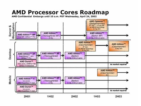
Looking at the geometric form of the CPU die, as well as the AMD roadmap, you can see that the Thoroughbred is only an intermediate step between the Palomino and the Barton. The dimensions and the rectangular form of the Thoroughbred's CPU die also make it clear that AMD has not only reduced the size of the die, but rearranged the individual units as well. Regarding the latter, this reduces efforts and does away with the need for a redesign when the L2 cache of the processor is increased in the near future. For this reason, AMD arranged the transistors differently for the L2 cache, with the goal of expanding the L2 cache to 512 kB.
With almost 54 million transistors, the new Barton die (successor to the Thoroughbred) thus catches up (at least in terms of numbers) with the Intel Pentium 4 and its 55 million transistors. Since the Barton is also based on a 0.13-µm process, the surface area of the CPU core increases from 80 mm² (Thoroughbred) to 115 mm² (Barton) .
Still, the surface area of the Barton core is significantly smaller than the 146 mm² required by the Intel Pentium 4 with the Northwood core. The bottom line is that the smaller CPU die allows the manufacturer to produce a larger number of processors from a single wafer, whereas Intel will increasingly be making use of 300 mm wafers in the future. AMD uses only silicon wafers with a diameter of 200 mm in its Fab 30 in Dresden, Germany.
The latest roadmap from AMD. In older versions, an Appaloosa core with a smaller die was also planned as the successor to the Morgan core.
Get Tom's Hardware's best news and in-depth reviews, straight to your inbox.
Current page: Exclusive Details On The Barton (Q3 2002)
Prev Page Heat Dissipation: All AMD-CPUs Compared Next Page Greater Yield: 322 Athlon-CPUs Per Wafer