ASML ships its second High-NA EUV litho tool to unspecified client

ASML
(Image credit: ASML)

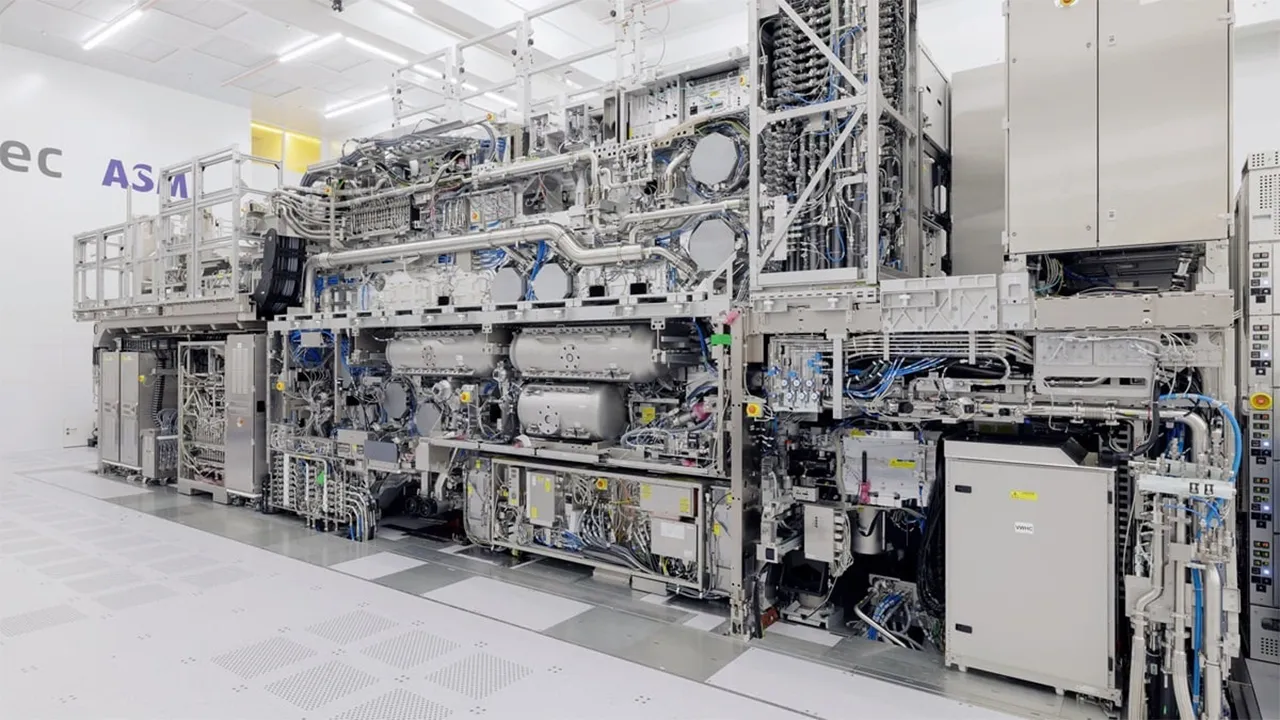
ASML on Wednesday said that it had begun to ship its second High-NA EUV lithography system to another customer. The announcement highlights that there is a major interest for next-generation extreme ultraviolet (EUV) lithography among leading chipmakers. Meanwhile, it is not clear which of ASML's customers is the second company to get an EUV tool with a 0.55 numerical aperture projection optics. 

"Regarding High-NA, or 0.55 NA EUV, we shipped our first system to a customer and this system is currently under installation," said Christophe Fouquet, chief business officer of ASML, at the company's earnings conference call with analysts and investors. "We started to ship the second system this month and its installation is also about to start."

ASML began to ship its first High-NA EUV litho tool — the Twinscan EXE:5000 — to Intel at the end of 2023. Intel will use the system to learn how to use such machines and will insert the system into mass production with its Intel 14A fabrication process, which is a few years away. By starting to work on its High-NA EUV-based process technologies early enough, Intel will be able to develop industry-standards for next-generation lithography, which is poised to become a competitive advantage in the coming years. 

"During the SPIE industry conference in February, we announced first light on our High-NA system located in our joint ASML-Imec High-NA lab in Veldhoven," said the CBO. "We have since achieved first images, with a new record resolution below 10nm and expect to start exposing wafers in the coming weeks. All High-NA customers will use this system for early access to process development."

While TSMC and Rapidus do not seem to be in hurry to adopt High-NA EUV lithography systems for mass production, they ill still have to do it sometime down the road, which is why ASML is optimistic about the future of this technology. In fact, the world's largest maker of wafer fab tools is exploring Hyper-NA, EUV lithography tools with projection optics featuring numerical aperture with higher than 0.7. 

"The customer interest for our [High-NA] system lab is high as this system will help both our Logic and Memory customers prepare for High-NA insertion into their roadmaps," said Fouquet. "Relative to 0.33 NA, the 0.55 NA system provides finer resolution enabling an almost 3x increase in transistor density, at a similar productivity, in support of sub-2nm Logic and sub-10nm DRAM nodes."

Anton Shilov
Freelance News Writer

Anton Shilov is a Freelance News Writer at Tom’s Hardware US. Over the past couple of decades, he has covered everything from CPUs and GPUs to supercomputers and from modern process technologies and latest fab tools to high-tech industry trends.

  • edzieba
    They also don't specific the customer for the first unit (known to be Intel), so this could just as well be a second unit to Intel as to anyone else.
    Reply
  • gg83
    edzieba said:
    They also don't specific the customer for the first unit (known to be Intel), so this could just as well be a second unit to Intel as to anyone else.
    That was my first thought as well. The only other company would be TSMC right? Or a research organization like imec?
    Reply
  • edzieba
    gg83 said:
    That was my first thought as well. The only other company would be TSMC right? Or a research organization like imec?
    Or any of the DRAM or NAND manufacturers. Or Samsung.
    Reply
  • gg83
    edzieba said:
    Or any of the DRAM or NAND manufacturers. Or Samsung.
    I didn't know dram and nand used bleeding edge transistor density.
    Reply
  • edzieba
    gg83 said:
    I didn't know dram and nand used bleeding edge transistor density.
    Nothing to do with transistors, DRAM and NAND are not fabbed by magic, but by the same equipment as CPUs or any other ICs. Narrower line-widths mean denser memory.
    Reply