Xilinx Starts Sampling 7nm Versal FPGA
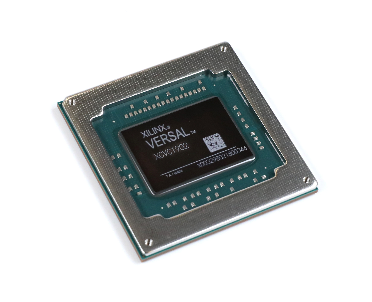
Xilinx announced that it had shipped samples of its next-generation 7nm Versal FPGA, or as the company would rather call it, the industry’s first adaptive compute acceleration platform (ACAP), and shared specifications. The company plans for a general launch in the second half of the year.
Xilinx says it has shipped the Versal devices, which taped out at the end of 2018, through its early access program to multiple Tier 1 customers. The first chips are from the Versal AI Core and Versal Prime series. Commenting on the milestone, Xilinx CEO Victor Peng said: “Having our first Versal ACAP silicon back from TSMC ahead of schedule and shipping to early access customers is a historic milestone and engineering accomplishment. It is the culmination of many years of software and hardware investments and everything we’ve learned about architectures over the past 35 years. The Versal ACAP is a major technology disruption and will help spark a new era of heterogeneous compute acceleration for any application and any developer.”
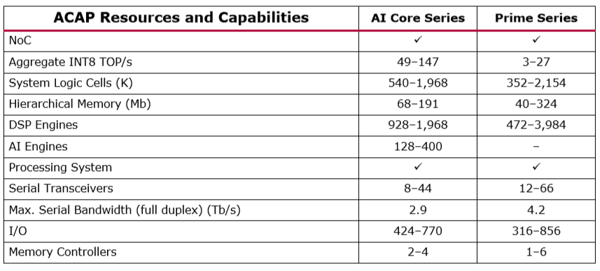
AI Core (PDF) is the initial high-end series, and it includes an AI Engine that delivers up to 133 TOPS of INT8 performance for additional number crunching capabilities that appeal to the deep learning inference market. The Prime series (PDF) is the company’s mid-range offering meant for a broad range of workloads and markets, with over two million logic cells, six DDR4 channels, and PCIe 4.0 support, but it lacks the AI Engine. The AI Core series only has four memory channels, and also only ~2000 DSPs compared to the Prime’s ~3000 DSPs. That provides the latter with up to 6.4 TFLOPS of FP32 performance and 27.5 TOPS of INT8 performance.
Xilinx's Versal line-up slots into the new ACAP product category it has invented. In this way, Xilinx wants to emphasize the adaptability of the platform, which in large part comes from the vast array of other IP on the heterogeneous platform beside the mere FPGA fabric, including an all-new VLIW-based AI Engine (as mentioned earlier) for machine learning inference and 5G workloads.
Over 1,500 employees have been working on this 7nm generation for over five years, and Xilinx says it has spent more than $1 billion on R&D. Xilinx’ own definition of ACAP reads: “An ACAP is a highly integrated, multicore, heterogeneous compute platform that can be changed at both the hardware and software levels to dynamically adapt to the needs of a wide range of applications and workloads in data center, automotive, 5G wireless, wired and defense markets.”
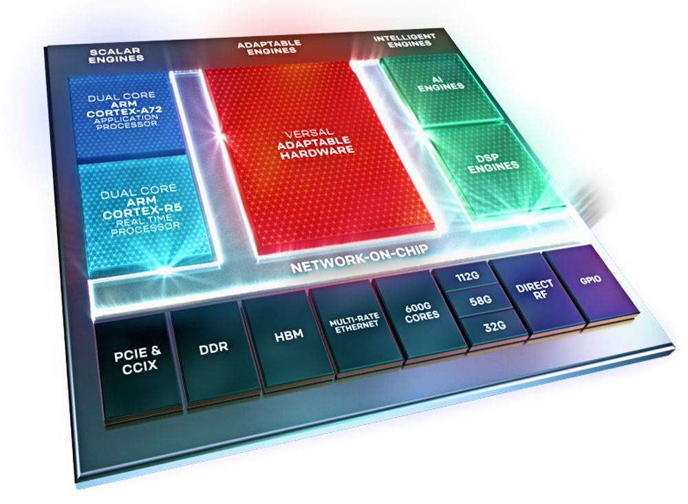
In other words, an ACAP is an almost universal accelerator that can be adapted in both hardware and software to the workloads it is used for. Xilinx classifies the accelerators within Versal as scalar engines (dual-core Cortex-R5F and Cortex-A72 real-time and application processors), adaptable engines (the FPGA fabric, which also provides an additional 31 TOPS of IN8 performance), and intelligent engines (DSP and AI Engines). All IP is connected via a 2.5Tb/s network-on-chip (NoC).
With the first samples having been sent to customers, Xilinx says that the AI Core and Prime series will be “generally available” in the second half of 2019. It is unclear if this means that the early access program is opening up to everyone, or if this refers to the official launch of the product, since at the 16nm generation it took the company well over a year for the devices to go from samples to launch. Since the tape-out happened at the end of 2018, we would be surprised to see a launch before the holidays. (Additionally, a design win in the FPGA world can generally take years to materialize. For instance, in the last quarter of 2018, Xilinx said that its 16nm volume had quadrupled year-over-year.
Get Tom's Hardware's best news and in-depth reviews, straight to your inbox.
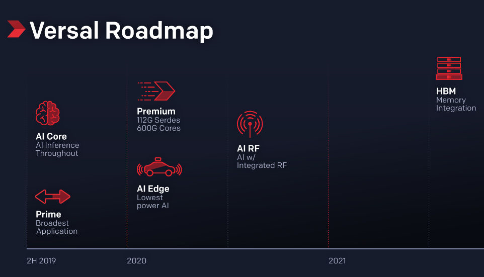
The AI Core and Prime series are the first two of six series on the Versal roadmap. In the first half of next year, the company plans to introduce the Premium series with 112G SerDes and the AI Edge series for low power inference at the edge. In the second half of 2020, the AI RF series will be available with integrated RF capabilities. The HBM series will ship a year later still, in the second half of 2021.
Versal is the 7nm successor to the company’s 16nm Virtex UltraScale+ FPGA family, which started sampling in late 2015, and it contains 50 billion transistors. Being first to the FinFET generation has given the company some key product wins in the last few years, such as the AWS F1 cloud instance. The company is the market share leader in FPGAs and saw strong revenue growth in the last year as 16nm volume increased significantly, with strength in automotive, data center, and communications.
Intel’s competitor, Stratix 10 on 14nm, is generally seen as having equal to better performance but started sampling a year later in late 2016. Nevertheless, Intel was first to market with 58G transceivers and integrated HBM. It recently disclosed plans for its 10nm Agilex platform that is similarly targeted at broad adaptability. Agilex is scheduled for first availability next quarter, but this most likely also refers to samples.
The full Versal whitepaper can be accessed here (pdf).
ACAP: What we Know so Far
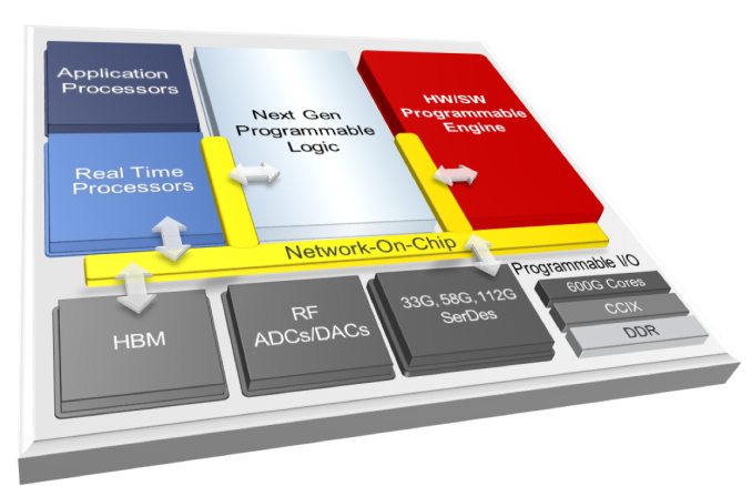
Taking a step back, Xilinx unveiled the ACAP early last year under the name Project Everest, shortly after it appointed Victor Peng as new CEO. Xilinx designed the platform under the company’s belief that Xilinx wasn’t just an FPGA company anymore since it was developing 3D chips, integrating full SoCs into the chips, and creating ecosystems and software frameworks. The concept was that Project Everest would combine its next-gen programmable logic with ARM application processors, real-time processors (Cortex-R5F), one or more HW/SW programmable engines (including DSP capabilities), high-bandwidth memory (HBM), RF converters, up to 112G SerDes, and programmable I/O such as DDR and the CCIX interconnect, and would come in both monolithic and interposer configurations.
These engines and interfaces would then be connected by a network-on-chip (NoC) that would aid the programmability of the platform, ultimately to make the hardware as agile as the software. The promised capabilities of being 10-100x faster and more efficient than CPUs and previous FPGAs in certain workloads (including ML inference and 5G), while also being more versatile than GPUs and ASICs in its number of use cases, still sounds a lot like what an FPGA is all about, but Xilinx classifies ACAP as a new product category that consists of a universal accelerator for both the edge and cloud. Xilinx says the configuration time of its ACAPs will be on the order of milliseconds, or almost ten times faster than current FPGAs.
In October, Xilinx was ready to announce the initial specifications and Versal branding and roadmap. There are four main series: Versal AI, Versal Prime, Versal Premium, and Versal HBM. The AI series, however, is further split into three lines: AI Edge, AI Core, and AI RF. Each series will only contain a subset of all available blocks in the block diagram. The high-end AI Core and mid-range Prime series are the first to come to market (in the second half of 2019), while Versal HBM won’t ship until the second half of 2021. Because of the cost of designing and manufacturing 7nm chips, there will be no low-end platform.
In terms of specifications, Xilinx separated the compute capabilities in three categories: scalar engines, adaptable engines, and intelligent engines. The scalar engines consist of a dual-core Cortex-A72 application processor and a dual-core Cortex-R5F real-time processor. The adaptable engine is the traditional FPGA fabric but also contains DSP slices. The DSP capabilities have been “significantly upgraded,” and now supports floating-point operations. In numbers, it has up to 29 TOPS INT8 throughput, but this quadruples with INT4 and quadruples again with INT2, and doubles to almost 1 TOPS of INT1 performance. Lastly, the intelligent engines are split into the AI Engine and DSP Engine.
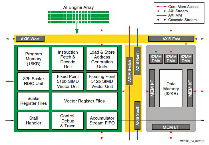
From a high level, the AI Engine consists of a tiled array of VLIW vector (SIMD) processors with 128-bit instruction words. Each tile contains both a scalar and a vector unit. The scalar unit contains a 32-bit RISC processor and a 32x32 multiplier with support for non-linear functions. The vector unit contains both a 512-bit integer and single-precision (FP32) floating-point unit. Each of these tiles is connected via the NoC.
The AI Core series features 128 to 400 of these AI Engine tiles, delivering up to 133 TOPS INT8 and 8 TFLOPS FP32 performance. The SRAM has a bandwidth of 66.5TB/s available. The DSP Engine, meanwhile, has a peak INT8 throughput of 13.6 TOPS. Put another way, INT8 can be done on the intelligent AI and DSP engines, for a total performance of 175.6 TOPS. INT8 is the only data format that can leverage all three engines, though. FP32 can be done on both the AI and DSP engines, but the other additional formats are unique to each engine.
The Prime series, on the other hand, does not have an AI Engine. Its intelligent engine has slightly higher integer throughput and circa 50% higher DSP throughput at 21.3 INT8 TOPS and 5.0 FP32 TFLOPS. It also features six memory controllers instead of four.
Versal further features support for PCIe Gen4x16, CCIX, DDR4 and LPDDR4. The NoC has a cross-sectional bandwidth of 2.5Tb/s and there are almost two million logic cells. Xilinx has not provided general performance (frequency), efficiency or TDP numbers yet.
Comparison to Agilex
While Xilinx touts Versal as the industry’s first ACAP product, Intel’s Agilex received a rather modest unveil in comparison, coming as merely a part of Intel’s broad data-centric launch event in early April. Although Intel did not adopt the ACAP product category name, we certainly think that it fits the category. As we covered back then, Agilex is in fact far more adaptable and hardware customizable than Versal due to the option to connect any possible chiplet via EMIB to the platform.
For example, while the initial F-series Agilex supports DDR4, PCIe Gen4, and 58G transceivers just like Versal, support for DDR5 and PCIe Gen5, CXL, Optane Persistent Memory, 112G transceivers and HBM will be added in later series by connecting appropriate chiplets to the monolithic base FPGA, which remains unchanged.
With regards to scalar engines, Intel has not talked about having real-time processors, but theoretically this could be added via a chiplet. The same goes for the application processor. The Versal series announced so far features two A72 cores. Intel has chosen to go for the simpler Cortex-A53, although there are four of them. However, one of the chiplet examples that Intel has given is an octa-core A7x series chiplet. Because it is a chiplet, there is no need for a respin of the silicon, and only those who need the faster ARM processor have to pay for it.
In terms raw of feeds and speeds, it is a bit of a give and take. Agilex delivers up 20 TFLOPS with FP32, the same as the Versal Prime series. However, Agilex also supports FP16, and even bfloat16, at twice the throughput. On the integer side, Intel’s FPGA tops out at 92 TOPS INT8, somewhat below the Versal AI Core which benefits from having a dedicated AI Engine. While Versal has support for INT1 up to INT16 in steps of powers of two, Agilex supports INT16 and INT8 though INT2 configurations.
It is unknown if Intel will add additional compute capabilities to Agilex akin to the AI Engine in the AI Core series, but it should be noted that Intel does have other products in its AI portfolio, most notably its Nervana product families for inference and training and also the Xe GPUs it is working on. Intel is often criticized for potentially spreading itself too thin in AI, but another way of viewing Intel’s portfolio is as a one-stop shop: while Xilinx will always have its heritage in FPGAs, NVIDIA in GPUs and Qualcomm, with their respective AI offerings hence being modifications of their core product, Intel is offering both dedicated AI capabilities with Nervana and the aforementioned modifications in its existing product lines under the DLBoost name.
So in short, Xilinx has chosen to create a multitude of series, each with its own silicon from mid-range to high-end and each with different IP blocks, while Intel is leveraging EMIB to be able to personalize the product with standard or custom tiles, starting from a strong monolithic base die. Both companies are similarly working on software frameworks to make their FPGAs as easily programmable as possible (for Intel via its OneAPI framework).
-
bit_user ReplyThe DSP capabilities have been “significantly upgraded,” and now supports floating-point operations. In numbers, it has up to 29 TOPS INT8 throughput, but this quadruples with INT4 and quadruples again with INT2, and doubles to almost 1 TOPS of INT1 performance.
The last one should be "almost 1 POPS" (short for Peta-Ops Per Second). Yes, it sounds like a lot, but keep in mind that these are probably just the most simple logic operations.
BTW, I've never heard anyone talk about INT1 - usually, it's referred to simply as bit-wise operations. I guess if they have a 1-bit add w/ carry, that would qualify it as something more than bit-wise. But, I rather doubt it.
