The History Of AMD CPUs
AMD K10: Fusion/Llano
AMD's Fusion project came to fruition in July 2011, when the company released its first APUs, code-named "Llano." The design combined a large number of AMD's Radeon Stream Processors based on the TeraScale 2 architecture with the company's K10 CPU cores. The underlying concept was similar to AMD's Geode line, which hadn't been updated in years. But where the Geode was designed as a low-power/performance solution, Llano was meant to be a higher-performance product.
It was never meant to compete in the high-end, but the idea was to create a SKU that could give reasonable CPU and graphics performance all in one. Llano suffered from a lack of L3 cache, and the iGPU was far too slow to keep most gamers happy, but for casual gamers that didn't mind lower graphics settings, it performed well enough.
AMD Llano
| Code Name | Llano |
|---|---|
| Date | July 2011 |
| Architecture | 64-bit |
| Data Bus | 64-bit |
| Address Bus | 64-bit |
| Maximum Memory Support | 1 TB |
| L1 Cache (Per Core) | 64 KB + 64 KB |
| L2 Cache (Per Core) | 1 MB (Full Speed) |
| L3 Cache (Shared) | None |
| Clock Speed | 2.1 - 3 GHz |
| Memory Controller | Dual-Channel DDR3-1866 |
| Core Count | 2, 3, 4 |
| SIMD | MMX, Enhanced 3DNow!, SSE, SSE2, SSE3, SSE4a |
| Fab | 32 nm |
| Transistor Count | 1,178 Million |
| Power Consumption | 65 - 100 W |
| Voltage | 0.45 - 1.4125 V |
| Die Area | 227 mm² |
| Socket | Socket FM1 |
| iGPU | TeraScale 2 (Radeon HD 5000, rebranded as Radeon HD 6000) |
AMD Bobcat
To be more competitive with Intel's Atom and ARM's low-power microprocessors, AMD introduced its Bobcat architecture in 2011. Since Bobcat was designed to be efficient, it ran at fairly low clock speeds; the highest-performing model reached 1.75 GHz. Bobcat is technically an APU, and it contains an iGPU with 80 Stream Processors based on the TeraScale 2 architecture. The iGPU is clocked rather conservatively as well in order to keep power consumption low.
Article continues belowAMD Bobcat
| Code Name | Desna, Ontario, Zacate |
|---|---|
| Date | 2011 |
| Architecture | 64-bit |
| Data Bus | 64-bit |
| Address Bus | 64-bit |
| Maximum Memory Support | 1 TB |
| L1 Cache (Per Core) | 32 KB + 32 KB |
| L2 Cache (Per Core) | 512 KB (Full Speed) |
| L3 Cache (Shared) | None |
| Clock Speed | 0.8 - 1.75 GHz |
| Memory Controller | Single-Channel DDR3L-1333 |
| Core Count | 1 - 2 |
| SIMD | MMX, SSE, SSE2, SSE3, SSSE3, SSE4a, SSE4.1/4.2, AVX |
| Fab | 40 nm |
| Transistor Count | N/A |
| Power Consumption | 4.5 - 18 W TDP |
| Voltage | 0.5 - 1.4 V |
| Die Area | 107 mm² |
| Socket | AM1 |
| iGPU Architecture | TeraScale 2 |
| iGPU Shader Count | 80 |
AMD Bulldozer: Zambezi
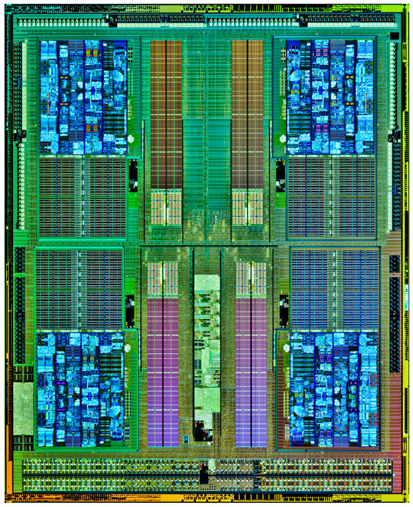
In October 2011, AMD introduced the successor to its K10 architecture, code-named "Bulldozer." With Bulldozer, AMD attempted to use high core count and clock speed to outperform Intel's recently-released Sandy Bridge. The cost of this clock rate-focused design, however, was a marked drop in IPC compared to the K10 architecture, and the design has been plagued with problems. The first Bulldozer chip, code-named Zambezi, was not able to cleanly out-perform Thuban Phenom II X6 CPUs, let alone beat Sandy Bridge. Part of the problem came from the use of a Multi-Core Module (MCM) that contains two integer cores and one FPU. As the two integer execution units have to share the FPU, this can lead to stalls in the pipeline.
The design has also been criticized for being power-hungry and running too hot, though that stems from direct comparisons between Bulldozer and Sandy Bridge.
AMD Bulldozer Zambezi
| Code Name | Zambezi |
|---|---|
| Date | October 2011 |
| Architecture | 64-bit |
| Data Bus | 64-bit |
| Address Bus | 64-bit |
| Maximum Memory Support | 1 TB |
| L1 Cache (Per Module) | 64 KB + (2 x 16 KB) |
| L2 Cache (Per Module) | 2 MB (Full Speed) |
| L3 Cache (Shared) | 8 MB |
| Clock Speed | 2.8 - 4.2 GHz (4.3 GHz Turbo) |
| Memory Controller | Dual-Channel DDR3-1866 |
| HyperTransport | 2600 MHz |
| Core Count | 4, 6, 8 |
| SIMD | MMX, SSE, SSE2, SSE3, SSSE3, SSE4a, SSE4.1/4.2, AVX |
| Instructions | AES, FMA4, XOP |
| Fab | 32 nm |
| Transistor Count | N/A |
| Power Consumption | 95 - 125 W |
| Voltage | 0.95 - 1.4125 V |
| Die Area | 316 mm² |
| Socket | AM3+ |
AMD Piledriver: Trinity And Richland
A year after Bulldozer debuted, AMD released a revised architecture known as Piledriver. Piledriver was initially released with Trinity, the company's second-gen APU. It saw clock speed increase by about 10 percent, and that, in conjunction with architectural enhancements, pushed performance up by roughly 15 percent without increasing power consumption.
On the iGPU side, Trinity moved to the TeraScale 3 architecture used inside of AMD's Radeon HD 6900-series GPUs. This helped to increase graphics performance over Llano.
Get Tom's Hardware's best news and in-depth reviews, straight to your inbox.
Richland, in turn, was a slightly improved Piledriver part. It performed just slightly better than Trinity due to higher clock speeds. It also managed to reduce power consumption and heat somewhat. The performance gap between mobile Trinity APUs and mobile Richland APUs was greater than on the desktop, owing to the improved thermals and power consumption.
AMD Trinity And Richland APUs
| Code Name | Trinity | Richland |
|---|---|---|
| Date | October 2012 | May 2013 |
| Architecture | 64-bit | 64-bit |
| Data Bus | 64-bit | 64-bit |
| Address Bus | 64-bit | 64-bit |
| Maximum Memory Support | 1 TB | 1 TB |
| L1 Cache (Per Module) | 64 KB + (2 x 16 KB) | 64 KB + (2 x 16 KB) |
| L2 Cache (Per Module) | 2 MB (Full Speed) | 2 MB (Full Speed) |
| L3 Cache (Shared) | - | - |
| Clock Speed | 2.9 - 3.8 GHz (4.2 GHz Turbo) | 2.1 - 4.1 GHz (4.4 GHz Turbo) |
| Memory Controller | Dual-Channel DDR3-1866 | Dual-Channel DDR3-2133 |
| Core Count | 2 - 4 | 2 - 4 |
| SIMD | MMX, SSE, SSE2, SSE3, SSSE3, SSE4a, SSE4.1/4.2, AVX | MMX, SSE, SSE2, SSE3, SSSE3, SSE4a, SSE4.1/4.2, AVX |
| Instructions | AES, BMI1, F16C, FMA3, FMA4, TBM, XOP | AES, BMI1, F16C, FMA3, FMA4, TBM, XOP |
| Fab | 32 nm | 32 nm |
| Transistor Count | 1,303 Million | 1,300 Million |
| Power Consumption | 65 - 100 W | 45 - 100 W |
| Voltage | 0.825 - 1.475 V | N/A |
| Die Area | 246 mm² | 246 mm² |
| Socket | FM2 | FM2 |
| iGPU | TeraScale 3 (Radeon HD 6900) | TeraScale 3 (Radeon HD 6900 - Rebranded As Radeon HD 8000) |
AMD Piledriver: Vishera
AMD also applied its Piledriver architecture to the FX family, displacing Zambezi in favor of Vishera.
AMD Bulldozer Vishera
| Code Name | Vishera |
|---|---|
| Date | October 2012 |
| Architecture | 64-bit |
| Data Bus | 64-bit |
| Address Bus | 64-bit |
| Maximum Memory Support | 1 TB |
| L1 Cache (Per Module) | 64 KB + (2 x 16 KB) |
| L2 Cache (Per Module) | 2 MB (Full Speed) |
| L3 Cache (Shared) | 8 MB |
| Clock Speed | 3.3 - 4.7 GHz (5 GHz Turbo) |
| Memory Controller | Dual-Channel DDR3-1866 |
| HyperTransport | 2600 MHz |
| Core Count | 4, 6, 8 |
| SIMD | MMX, SSE, SSE2, SSE3, SSSE3, SSE4a, SSE4.1/4.2, AVX |
| Instructions | AES, BMI1, F16C, FMA3, FMA4, TBM, XOP |
| Fab | 32 nm |
| Transistor Count | N/A |
| Power Consumption | 95 - 125 W (220 W) |
| Voltage | 0.875 - 1.425 V |
| Die Area | N/A |
| Socket | AM3+ |
AMD Steamroller: A GCN APU
In 2014, AMD updated its APU line again with the new Steamroller architecture. AMD shifted to a new 28nm process that favored chip density over clock speeds in order to be more compatible with its graphics technology. The CPU demonstrated a reasonable increase in IPC over its predecessor, thanks in part to a larger L1 cache and additional internal registers. It wasn't able to hit the same clock speeds as Richland though, so overall performance didn't increase much.
The graphics side of the APU improved drastically, however, owing to the new transistor technology, an increase in shader count, and a move to AMD's GCN GPU architecture. The APU featured a number of other enhancements, such as being the first HSA-compatible APU, the addition of AMD's TrueAudio DSP technology and support for PCIe 3.0.
The first Steamroller APUs use a configuration known as Kaveri. The APU line was later refreshed with Godavari, which benefits mostly from higher clock speeds.
| Code Name | Kaveri | Godavari |
|---|---|---|
| Date | January 2014 | May 2015 |
| Architecture | 64-bit | 64-bit |
| Data Bus | 64-bit | 64-bit |
| Address Bus | 64-bit | 64-bit |
| Maximum Memory Support | 1 TB | 1 TB |
| L1 Cache (Per Module) | 96 KB + (2 x 16 KB) | 96 KB + (2 x 16 KB) |
| L2 Cache (Per Module) | 2 MB (Full Speed) | 2 MB (Full Speed) |
| L3 Cache (Per Module) | None | None |
| Clock Speed | 3.1 - 3.7 GHz (Turbo 4 GHz) | 2.9 - 3.9 GHz (Turbo 4.1 GHz) |
| Memory Controller | Dual-Channel DDR3-2133 | Dual-Channel DDR3-2133 |
| Core Count | 2 - 4 | 2 - 4 |
| SIMD | MMX, SSE, SSE2, SSE3, SSSE3, SSE4a, SSE4.1/4.2, AVX | MMX, SSE, SSE2, SSE3, SSSE3, SSE4a, SSE4.1/4.2, AVX |
| Instructions | AES, BMI1, F16C, FMA3, FMA4, TBM, XOP | AES, BMI1, F16C, FMA3, FMA4, TBM, XOP |
| Fab | 28 nm | 28 nm |
| Transistor Count | 2.41 Billion | N/A |
| Power Consumption | 65 - 95 W | 65 - 95 W |
| Voltage | N/A | N/A |
| Die Area | 245 mm² | N/A |
| Socket | FM2+ | FM2+ |
| iGPU | GCN Radeon R5/R7 | GCN Radeon R5/R7 |
AMD Jaguar
AMD introduced its Jaguar architecture in 2014 to replace the aging Bobcat core. Jaguar increased the CPU core count to four and moved to a faster GCN-based graphics processor with 128 shaders. IPC shot up by roughly 15 percent as well, alongside a boost in clock speed. Overall, Jaguar is significantly faster than Bobcat in every way.
The Jaguar architecture in also used inside of the Xbox One and Playstation 4. The models inside of these game consoles have significantly higher core counts on both the CPU and iGPU, however, and Jaguar-based products available in other devices are considerably slower.
AMD Jaguar
| Code Name | Kabin, Temash |
|---|---|
| Date | April 2014 |
| Architecture | 64-bit |
| Data Bus | 64-bit |
| Address Bus | 64-bit |
| Maximum Memory Support | 1 TB |
| L1 Cache (Per Core) | 32 KB + 32 KB |
| L2 Cache (Per Core) | 512 KB (Full Speed) |
| L3 Cache (Shared) | None |
| Clock Speed | 1.3 - 2.05 GHz |
| Memory Controller | Dual-Channel DDR3-1600 |
| Core Count | 2 - 4 |
| SIMD | MMX, SSE, SSE2, SSE3, SSSE3, SSE4a, SSE4.1/4.2, AVX |
| Fab | 28 nm |
| Transistor Count | N/A |
| Power Consumption | 3.9 - 25 W TDP |
| Voltage | 0.5 - 1.4 V |
| Die Area | 107 mm² |
| Socket | AM1 |
| iGPU Architecture | GCN Radeon R3 |
| iGPU Shader Count | 128 |
Excavator: The End Of Bulldozer
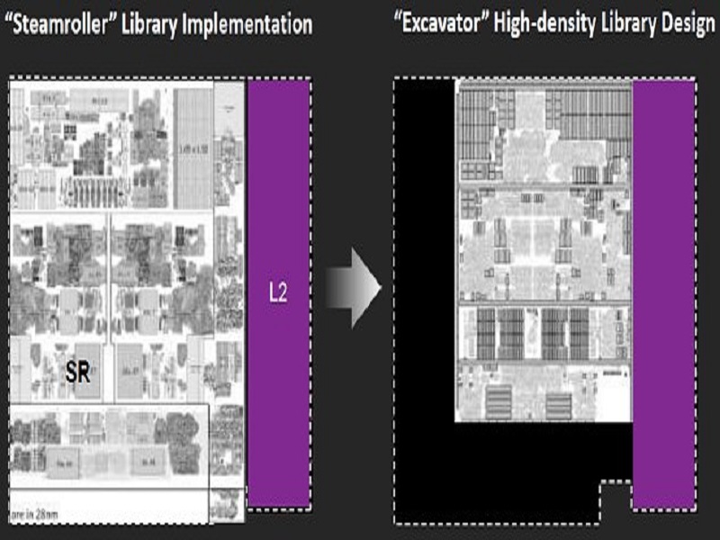
The last architecture that AMD plans to produce based on Bulldozer is known as Excavator, which is used inside of AMD Carrizo-based APUs. Relatively few of these products have been released thus far, so we can't be sure what the clock speed limit will be on these parts. Carrizo is designed to have significantly higher transistor density (than prior Bulldozer-based processors), which helps to reduce the die area and lower power consumption. AMD reworked the cache inside of Excavator, too.
The processor has less L2 cache, but twice as much L1 cache when compared to Steamroller. Because the L1 cache is several times faster than the L2 cache, this helps to boost IPC performance. The branch prediction target buffer was increased by 50 percent as well, to 768 KB, which further helps to improve performance. The graphics processor also gained 512 KB of dedicated L2 cache to increase graphics processing power. Rearranging the cache on the APU also helped to lower the power consumption, as cache tends to be fairly power hungry, and this new configuration has less overall cache on die.
AMD Excavator
| Code Name | Carrizo |
|---|---|
| Date | 2015 |
| Architecture | 64-bit |
| Data Bus | 64-bit |
| Address Bus | 64-bit |
| Maximum Memory Support | 1 TB |
| L1 Cache (Per Module) | 192 KB + (2 x 32 KB) |
| L2 Cache (Per Module) | 1 MB (Full Speed) |
| L3 Cache (Shared) | None |
| Clock Speed | 3.5 GHz (Athlon X4 845, Carrizo clock speed range unknown) |
| Memory Controller | Dual-Channel DDR3 |
| Core Count | 2 - 4 |
| SIMD | MMX, SSE, SSE2, SSE3, SSSE3, SSE4a, SSE4.1/4.2, AVX |
| Fab | 28 nm |
| Transistor Count | N/A |
| Power Consumption | 65 W TDP (Athlon X4 845, Carrizo power consumption range unknown) |
| Voltage | N/A |
| Die Area | N/A |
| Socket | FM2+ |
| iGPU Architecture | GCN Radeon R3 |
| iGPU Shader Count | 512 |
Ryzen: AMD Reborn
AMD lost ground to Intel in essentially every area of the CPU market during the Bulldozer years. The company lost significant financial resources and had to sell its silicon fabs. With an uphill battle to remain in the processor market, AMD put its hopes on Ryzen.
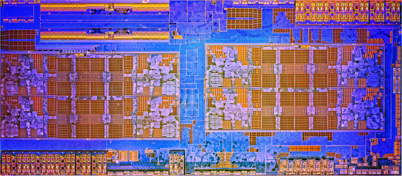
The top end Ryzen processor, Ryzen 7 1800X, has eight CPU cores clocked at 3.6 GHz. The CPU can also accelerate up to 4.1 GHz in certain work loads. The eight cores are organized into two partitions. Each partition has 8MB of L3 cache, and each core has a dedicated 512KB L2 cache, a 64KB L1 instruction cache, and a 64KB L1 data cache. This gives the Ryzen 7 1800X a total of 16MB of L3, 4MB of L2, and 1MB of L1 cache.
In Ryzen, AMD implemented its first micro-op cache, which can store recently used instructions, improving performance and reducing pipeline stalls. Ryzen processors also support Hyper-Threading, which allows cores to handle two threads simultaneously. The company's processor debuts alongside the new AM4 socket, adding support for DDR4 RAM.
Ryzen 7 was closely followed up by its Ryzen 5 processors, which are created from semi-defective Ryzen 7 cores. Ryzen 5 is available in quad- and hexa-core variants and at similar clock speeds to Ryzen 7.
AMD Ryzen
| Code Name | Ryzen |
|---|---|
| Date | 2016 |
| Architecture | 64-bit |
| Data Bus | 64-bit |
| Address Bus | 64-bit |
| Maximum Memory Support | 1 TB |
| L1 Cache | 64KB L1 I + 64KB L1 D |
| L2 Cache | 512KB |
| L3 Cache (Shared) | 8MB |
| Clock Speed | 3.6GHz |
| Memory Controller | Dual-Channel DDR4 |
| Core Count | 4 - 8 |
| SIMD | MMX, SSE, SSE2, SSE3, SSSE3, SSE4a, SSE4.1/4.2, AVX |
| Fab | 14nm |
| Transistor Count | N/A |
| Power Consumption | 95W TDP |
| Voltage | N/A |
| Die Area | N/A |
| Socket | AM4 |
| iGPU Architecture | None |
| iGPU Shader Count | None |
MORE: Best CPUs
MORE: Best CPU Cooling
MORE: Intel & AMD Processor Hierarchy
MORE: All CPU Content
-
wurkfur ReplyThe eternal underdog will once more have his day.
How can you say eternal? For a good while AMD was actually making faster and more innovative stuff than Intel.
AMD launched dual cores for consumers
AMD integrated memory controllers on die
AMD created x64 versus Intel pushing the move to a new architecture that only they could make
AMD also pushed APU's mainstream
Intel adopted all these practices after the fact while engaging in illegal monopolistic behavior in an international stage that stifled innovation, cost jobs, and caused consumers to pay more.
One could argue that if Intel had simply played by the rules locally and abroad, AMD would have had enough cash flow to maintain their position through better R&D instead of playing catch up.
For that very reason I look forward to AMD's upcoming products to replace my 1090t that's clocked within an inch of its life. -
vern72 ReplyAMD launched dual cores for consumers
AMD integrated memory controllers on die
AMD created x64 versus Intel pushing the move to a new architecture that only they could make
AMD also pushed APU's mainstream
And one more thing: AMD was the first to ship a 1Ghz x86 CPU to the masses. -
CaedenV Fantastic article! Especially loved seeing the early chips; I had no idea that they were in the game pre 286 generation. I was a kid at the time and my understanding was that the law suits at the time were what allowed AMD (and Via... don't forget the 'true underdog' lol) to ENTER the market, not remain in it.Reply
Also, I remember endless debates when I built my first PC for college ~2001. I wanted an AMD XP chip... but my video editing software had issues with it (some sort of audio processing bug. Then it was between the Pentium 4 which had great burst performance, but terrible sustained performance due to RDRAM that could not keep up; and the Pentium 3 which looked terrible on paper and was 'old', but had fantastic sustained performance (and much healthier thermals!). In the end I decided on the Pentium 3, but (noob build mistake) because I bought a crap PSU it died within a year and I moved to my one and only AMD build which was a 2GHz Barton. That was a great PC that lasted a solid 3 years.
I was really sad to watch Bulldozer fall apart. After the Core2Duo AMD was falling behind and bulldozer was supposed to bring them back into relevance. But then the marketing department thought that nobody would buy a high-end $500+ CPU, so they slashed the cache to make it more affordable. Sadly that cache was needed to prevent the CPU from constantly going back to the system memory for instructions and it literally killed the product. And Intel happily sold several $400-1000 i7 chips while AMD could not even hold onto the budget market. Sad times. It is a shame that they were not able to sell the full chip as originally designed, and then cut down a cheap version for 'consumers'.
But now it looks like AMD is starting to play ball again. Next 3 years will be interesting to watch, and if they make a winner then I might throw my hat in their ring again when I do a rebuild 2-4 years from now. I would love to see something blow my 4.2GHz Sandy Bridge out of the water! -
CaedenV ReplyOld CPUs are so much... cooler than new ones.
you kidding? Those old chips ran meltingly hot! And with tons of power! when those old chips were OC'd they could drink down nearly 200W and easily heat a dorm room on cold winter nights! -
turkey3_scratch Reply17879424 said:Old CPUs are so much... cooler than new ones.
you kidding? Those old chips ran meltingly hot! And with tons of power! when those old chips were OC'd they could drink down nearly 200W and easily heat a dorm room on cold winter nights!
To be fair we have current GPUs on the market above 300W.
But by "cool" I just meant "cool" as in "vintage". -
SinxarKnights It is amazing to think that my old 433Mhz Intel processor was pretty good at the time. With 256MB of RAM the OS (Win98SE) was very responsive. The motherboard didn't have an AGP slot so I had to settle for a Nvidia GeForce FX 5200 from Wal-mart. Still have lots of fond memories of Diablo and Ultima Online.Reply
I built a PC with an Athlon 64 X2 5600+. Due to the larger cache, it gave a significant performance increase over the other lower tiered CPUs. This was right at the time Intel came out with the Core architecture. While the top end 64 X2 series (6000+ and up) outperformed the first Core CPUs that were released, everything went downhill from there for AMD.
15 years ago my awesome 433mhz CPU was awesome, today it cannot perform the most basic of task in a timely manner. I imagine 15 years from now my current 4790k will be in the same boat. -
Zachary Singer-Englar I still brag about my Athlon II x250 Regor. That was a great processor for an underfunded enthusiast, It shipped at 3.0 and i had it clocked to 3.5 for about 2 years on a stock cooler before I replaced the whole set-up because my motherboard gave out (probably unrelated to my overclocking). That was 5 years after I had purchased the processor. My FX-6350 is not holding up quite as well.Reply
