Introduction
It's not very long until the first AGP systems will hit the market. Intel will release its new 440LX Pentium II chipset with AGP support on August 26, 1997, only a few weeks away. Lots of hopes and hypes about AGP can be found all over the place and so I found it was time to add my 2 cents to this discussion, hopefully giving you some clear facts about this new interface.
What Does AGP Do?
AGP is nothing mystical at all and the idea behind AGP isn't even particularly unique. If future graphic accelerators should be particularly faster than the current PCI graphic cards it will take much more than just AGP. However AGP enables graphics hardware to do its job faster whilst also keeping the costs low.
The AGP specification is based on the 66 MHz PCI specification rev. 2.1, which isn't in much use currently, since all current PCI cards are still only able to use the 33 MHz PCI bus speed. AGP however is adding three special extensions via so called 'sideband' signals, provided by some special lines added to the PCI specs. These three extensions are
Article continues below- pipelined memory read/write operations
- demultiplexing of address and data on the bus
- timing for data transfer rate as if clocked with 133 MHz
Now what does this mean in laymen terms?
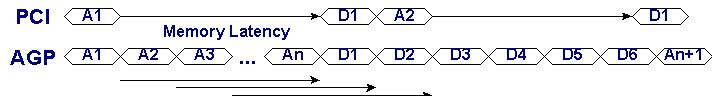
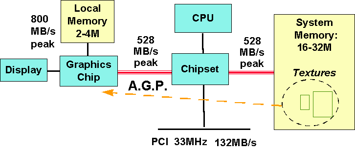
First of all AGP offers a much higher throughput over the AGP bus than PCI does. PCI as currently clocked at 33 MHz can transport 133 MB/s at peak rates over its 32 bit data bus (33,000,000 * 4 Byte * sec-1 ). AGP is clocked with 66 MHz, which enables a peak rate of 266 MB/s (66,000,000 * 4 Byte * sec-1 )at the classic so called 'x1' mode, but using the 'x2' mode, which transports data on both the rising and the falling edges of the 66 MHz clock, it can transport up to 532 MB/s at peak rate (please note that it is up to the graphic accelerator's vendor if 'x2' mode is supported). So far about the '133 MHz' data transfer rates, which doesn't mean that the AGP bus is clocked at 133 MHz at all! Now in real world AGP is able to transfer closer to the hypothetical peak values due to some extra signal wires which enable pipelining and queuing of requests.
Due to this new technology, AGP peak transfer rate is as high as the peak transfer rate of current main memory, which in Pentium and above systems operates with a 64 bit wide bus at 66 MHz bus clock. Future systems will reach a main memory peak transfer rate of 800 MB/s by using 100 MHz bus clock.
Now this new main memory like high data transfer rate that AGP offers us is only one part of the story, but for the beginning of AGP it might be the most important one.
Due to the high data transfer rate between the graphics accelerator and main memory, AGP enables graphic accelerators to use main memory instead of local memory for things like typically textures, which can be as big as up to 128 kB. These textures so far had to be loaded into the local graphic accelerator memory to be processed there by the graphic processor. Now these textures can be processed in main memory without a performance impact. Intel calls this DIME , for DI rect M emory "E xecute". UMA the 'unified memory architecture' used on low cost boards in the past, where already main memory was used as graphics memory, had two important differences:
- The main memory provided via AGP and thus called 'AGP memory' doesn't replace the screen buffer of the graphic accelerator as done in UMA. The AGP memory is an addition to it.
- UMA had to go through the much slower PCI interface.
These two differences show why UMA was particularly slow and should make you understand why AGP graphic accelerators should be faster than current PCI solutions.
If this is hard to understand, let me give you a simple example:
The 3D accelerators with the 3Dfx Voodoo chip e.g. the Diamond Monster 3D usually come with 4 MB memory. Now 2 MB of this memory are used for textures and 2 MB are used for frame buffer and Z-buffer. This is why the Monster 3D is limited to 640*480 resolutions in e.g. GLQuake, since only 2 MB can be used for frame buffering and 2 MB are used for textures, which would not be necessary if main memory could be used for this job, as possible with AGP's DIME.
"Graphics local RAM is usually more expensive than generalized system memory and it cannot be used for other purposes by the OS when unneeded by the graphics of the running applications. The graphics chip needs fast access to local memory for screen refresh, Z-buffers, and pixels (front and back-buffers). For these reasons, programmers can always expect to have more texture memory available via AGP system memory. Keeping textures out of the frame buffer allows larger screen resolution, or permits Z-buffering for a given large screen size. Most applications could use 2-16 MB for texture storage. By using AGP and DIME, they can get it." (Intel Corporation)
But let's for now get back to the theory again.
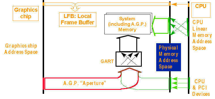
The chipset has to provide the function to map the 'AGP memory' to normal main memory. Intel calls this GART (Graphics Address Remapping Table).
"The processor "linear" virtual addresses get translated by its paging hardware into physical addresses. These physical addresses are used to access system RAM, local Frame Buffer, and AGP RAM. The CPU accesses to the Local Frame buffer and AGP RAM use the same addresses as the graphics chip does; for that reason, the operating system sets up the CPU paging hardware to a straight 1:1 non-translation of virtual to physical address. " (Intel Corporation)