Intel Outs Goldmont Plus Architecture Enhancements
Intel has released details of its Goldmont Plus microarchitecture. The design has several major advancements that boost performance and could lay the groundwork for more core-heavy designs in the future. For now, the revamped low-power cores will help Intel fend off the rise of Qualcomm's ARM-powered Windows 10 devices.
Intel recently released its Gemini Lake architecture with the Pentium and Celeron Silver SOCs. Intel announced the new processors with little aplomb or detail, and follow up questions helped us ferret out a few of the more obvious enhancements to the design. However, the details of the underlying Goldmont Plus microarchitecture, which has a deceivingly similar name to the Goldmont cores, eluded us.
Intel claims to have wrung impressive performance improvements from Gemini Lake, which features the Goldmont Plus cores, but with the same 14nm process found on its predecessor. That hints that the company made major architectural improvements, and now that Intel has refreshed its Architectures Optimization Reference Manual, it's clear the company has taken a huge step forward with the Goldmont Plus microarchitecture.
Goldmont Plus CPU Core Pipeline
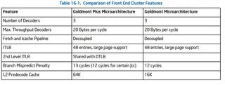
The enhanced Goldmont core comes with plenty of improved features. Intel expanded Goldmont's back-end pipeline from a 3-way allocation/retire to a 4-wide allocation/retire alignment, but the design inherits its predecessors' 3-wide fetch and decode pipeline. The microarchitecture also features an enhanced branch prediction unit and Intel bulked up the shared second level pre-decode cache from 16KB to 64KB.

Other improvements include a wider integer execution unit. This includes a load/store scheduler, three ALU schedulers, and a new dedicated JEU (Jump Execution Unit) port that supports faster branch prediction. Intel also expanded the load/store buffers, although the document does not provide specifics. A larger reservation station (scheduler) and expanded re-order buffer entries also support a larger out-of-order window. Intel also employs a Radix-1024 floating point divider for "fast scalar/packed single, double and extended precision floating point divides," along with paging cache enhancements.
Intel also added a shared second-level instruction and data TLB (Translation Lookaside Buffer; seen as ITLB and TLB on the graphics). The previous-gen architecture only supported data cache on the second-level TLB. Intel also made paging cache enhancements. There is also a slight uptick in the branch mispredict penalty to 13 cycles.

Perhaps one of the largest changes is a shift to a modular design that features quad-core clusters that share 4MB of L2 cache. That design could allow the company to simply add more clusters to build out larger processors with heftier core counts.
Stay on the Cutting Edge
Join the experts who read Tom's Hardware for the inside track on enthusiast PC tech news — and have for over 25 years. We'll send breaking news and in-depth reviews of CPUs, GPUs, AI, maker hardware and more straight to your inbox.
It might seem counter-intuitive to build large Atom-class processors, but pairing the enhanced performance with a low-power modular chip design could prove useful as Intel seeks to fend off newly-resurgent ARM competitors in the data center. The current design could help Intel grapple with the pending influx of Qualcomm-powered Windows 10 ARM devices, so the improved microarchitecture could serve Intel well on multiple fronts.
Intel is notably late with its 10nm process, and many predict the company will not release a new microarchitecture until Ice Lake, so the newly-revamped Goldmont is a positive development. The improvements to the Goldmont Plus microarchitecture are impressive, and curiously understated by Intel; we typically see more fanfare when the company makes big advances. There have already been new devices spotted with Gemini Lake in the wild, so we expect to see several new models wielding the Gemini Lake SoC at CES.

Paul Alcorn is the Managing Editor: News and Emerging Tech for Tom's Hardware US. He also writes news and reviews on CPUs, storage, and enterprise hardware.
-
bit_user Reply
Nice digging, Paul. Thanks for the update.20535543 said:now that Intel has refreshed its Architectures Optimization Reference Manual, it's clear the company has taken a huge step forward with the Goldmont Plus microarchitecture
Given that Goldmont was already appearing in entry-level laptops, I wish we could see some benchmarks to know how they compare with Intel's big cores on games and other apps interesting readers of this site.
-
Nintendork In mobile land no one gives a fluck duck about intel chips. It only was a tiny bit relevant when intel had to pretty much give them for free to some chinese OEM's in order to artifially get marketshare, they failed miserably, and the chips for free program was axed.Reply
Sin Zen scale so down so well in efficiency when you relax the frequencies, the major threat for cheap laptops/tablets to the ARM+win10 combo is the Ryzen 2c/4t 128-256 Vega SP APU's with <10w TDP. -
bit_user Reply
Yes, they did quite poorly in the cell phone market, but these aren't cell phone SoCs. Intel sells lots of these into entry-level laptops and Chromebooks.20541025 said:In mobile land no one gives a fluck duck about intel chips. It only was a tiny bit relevant when intel had to pretty much give them for free to some chinese OEM's in order to artifially get marketshare, they failed miserably, and the chips for free program was axed.
This is 1.5 generations newer than the cores they used in mobile. Aren't you at least curious to see how they compare to Intel & AMD desktop cores?20541025 said:Zen scale so down so well in efficiency when you relax the frequencies, the major threat for cheap laptops/tablets to the ARM+win10 combo is the Ryzen 2c/4t 128-256 Vega SP APU's with <10w TDP.
We can speculate all we want, but data is king. I say let's have some benchmarks!
Most Popular


