Microsoft HoloLens: HPU Architecture, Detailed
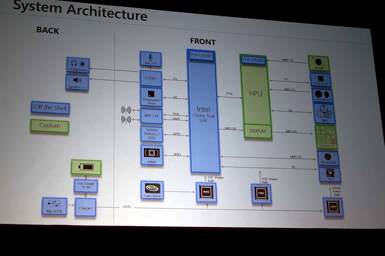
Earlier this week, we published our first look inside of Microsoft’s HoloLens and explained how the HMD works. Given the novel applications it enables, we were fairly amazed that the system architecture diagram presented at Hot Chips shows so much off-the-shelf hardware inside the wearable Windows 10-based platform. We were also intrigued by the custom components required to complete Microsoft’s vision of augmented reality, in particular the Holographic Processing Unit (HPU).
Essentially, the HPU is a vision processor (not unlike this one), and it’s designed as a companion to the SoC, handling tasks such as receiving all of the myriad sensor data, packaging that data, and feeding it to the SoC. That’s a simple summation of what it does, but we’re interested in how it works, by looking at the architecture of the HPU.
What’s The SoC?
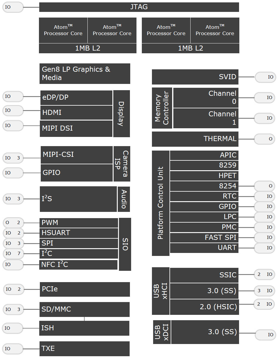
Although the company hasn't specified exactly which Atom SoC it uses for the primary computing functions of the HoloLens, Microsoft did say that it uses Intel’s Cherry Trail SoC. All of the processors in that family feature four out-of-order Airmont cores manufactured at 14 nm. Also worth noting is that Microsoft’s diagram shows the host SoC connecting to two devices via PCIe: the 802.11ac WiFi/BT 4.1 LE controller and its own HPU. Only one of Intel’s two Cherry Trail packages offers a pair of PCIe ports, pointing to the more complex 289 mm² Type 4 version.
Article continues belowAt least on paper, this configuration is available with up to 16 of Intel’s eighth-gen execution units for graphics, though there are also 12-EU SKUs. HD Graphics includes hardware-accelerated HEVC decode and H.264 encode support as well, which should help minimize power use during media playback tasks. And by stacking 1 GB of LPDDR3 memory in a package-on-package arrangement, Microsoft saves precious motherboard space.
Beyond its capable IA cores, Cherry Trail also hosts plenty of I/O that comes in useful for HoloLens. An integrated low-power engine enables encode/decode of audio streams to the built-in speakers and from the headset’s four microphones. Plenty of I²C interfaces make it easy to tack on temperature sensors and an ambient light sensor. Further, a MIPI-CSI attaches the 2 MP photo/HD video camera to Intel’s SoC. Finally, you’ll find 64 GB of flash connected via SDIO to Cherry Trail’s storage control cluster.
The HPU Architecture
But of course, HoloLens does require a handful of custom-made components, including the batteries, the displays, the depth sensors, and the HPU, which is key to aggregating environmental and gesture data before it gets to Intel’s SoC. Naturally, a lot of analysis went into determining what HoloLens’ HPU needed to do and what it would take to get there. The company explored heterogeneous compute across CPUs and GPUs, along with more traditional licensed cores. Eventually, though, Microsoft settled on a hybrid approach that employs programmable units wherever possible and fixed-function elements where they made sense.
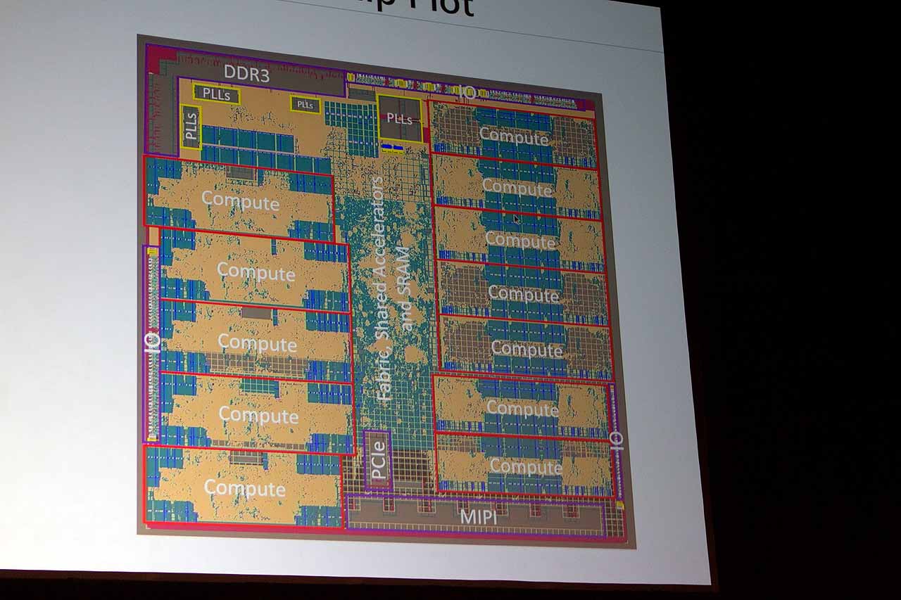
The resulting component is manufactured on TSMC’s 28 nm high-performance compact mobile computing process, optimized for low power and more compact layout. It measures 144 mm² and includes ~65 million logic gates.
Get Tom's Hardware's best news and in-depth reviews, straight to your inbox.
Most of the die area is consumed by 12 of what Microsoft calls “compute nodes”, each of which hosts two Tensilica configurable DSP cores (for a total of 24 cores). The company buillt upon Cadence’s Xtensa base instruction set with somewhere around 300 of its own extensions to stream input from the headset’s various subsystems, manipulate it, and pass the computed output in a compact format to the host SoC. Initially, Microsoft didn’t want any one compute node utilized more than 50%, so there should be plenty of headroom built into the HPU for more taxing algorithms, thereby future-proofing the HoloLens as much as possible.
The company also specified exacting latency and duty cycle requirements, intended to reasonably assure the best experience possible. To achieve this, operations that can’t be satisfactorily addressed by the DSP cores are handled with fixed-function accelerators. In much the same way as AMD and Nvidia dedicate some of their GPU transistor budget to specific tasks like decoding video or tessellating geometry, Microsoft implemented standalone accelerators and blocks of hardware tightly coupled with the DSP cores to speed up performance-critical operations. This combination facilitates somewhere in the neighborhood of one trillion pixel operations per second, yielding up to 200x improvement over a software-only implementation.
Wedged in between the compute nodes is 8 MB of SRAM, and like the Cherry Trail SoC, Microsoft’s HPU has 1 GB of package-on-package LPDDR3 memory. All around the HPU, serial interfaces enable communication with subsystems that feed into the HPU. The MIPI Alliance’s CSI, for instance, is used to collect input from the depth camera and four environment understanding cameras. MIPI-DSI connects the two displays. HoloLens’ inertial measurement unit (IMU) attaches to the HPU via SPI. A temperature sensor is enabled through an I²C interface, similar to the Cherry Trail chip.
Again, the HPU and Intel SoC communicate over PCI Express. According to Intel’s Atom Z8000 datasheet, Cherry Trail exposes two root ports at up to 5 GT/s. That would be a maximum of 500 MB/s between the components, if this holds true. Unfortunately, Microsoft won’t confirm our suppositions about PCIe, nor any of the SoC’s other specifications for that matter. So, we’re connecting a lot of dots based on the claims it is willing to make. Should additional details emerge, we’ll update accordingly.
-
wifiburger yes finally some information on their product, we all know people have to know what's inside this turd ! that's what sells it and makes Microsoft money NOT !Reply -
bit_user Thanks for the update.Reply
Initially, Microsoft didn’t want any one compute node utilized more than 50%, so there should be plenty of headroom built into the HPU for more taxing algorithms, thereby future-proofing the HoloLens as much as possible.
In order to satisfy realtime latency requirements, they need to leave some headroom. So, they can't just double the workload and still hit their latency targets.
The company also specified exacting latency and duty cycle requirements, intended to reasonably assure the best experience possible.
To me, the 1 GB of for the Atom cores seems like the weakest spec. This thing has to run Windows 10, their graphics stack, their AR stack, and the AR app, itself. For all that, 1 GB seems tiny.
-
alextheblue Bit - the HPU does a lot of the heavy lifting and that has it's own RAM. Also although it's running Win10, it's not configured the same. The memory footprint is greatly reduced, anything not needed isn't running.Reply -
bit_user Reply
Even if you strip down Win 10 to the minimum, once you add back in the stuff needed for AR + apps, it seems like 1 GB ought to be a squeeze.18523611 said:Bit - the HPU does a lot of the heavy lifting and that has it's own RAM. Also although it's running Win10, it's not configured the same. The memory footprint is greatly reduced, anything not needed isn't running.
I'm confident they'll add more RAM, in the next version. Maybe that'll even be something I can afford!
Hopefully, it'll also use Broxton, based on Intel's Goldmont core, which is allegedly 50% faster per clock. That also has Gen9 HD Graphics (up to 18 EUs, I think).


