Samsung Plows Forward With 11nm FinFET, 7nm EUV On Track For 2018
The pace of Moore's Law is slowing, and the bulk of the blame lies with optical lithography. EUV (Extreme Ultraviolet Lithography) technology should fix that, but the development effort that began back in the late '90s has been plagued by reliability and power consumption hurdles. Now that EUV tools are ready for the major fabs, Samsung, TSMC, Global Foundries, and Intel are all racing to the EUV finish line.
Samsung plans to lead the EUV charge with 7nm products slated for the second half of 2018, while its competitors will deploy production-class EUV in the 2020 timeframe. Of course, lithography naming conventions have turned into more of a marketing exercise than an actual quantifiable metric, and many predict that Samsung's 7nm is more akin to Intel's pending 10nm node.
Samsung began EUV testing in 2014 and claims to have processed over 200,000 wafers with the new technology. It also claims to have achieved an 80% yield rate for 256Mb SRAM (Static Random-Access Memory) chips with EUV, but notably, doesn't indicate the process node.
Samsung's and Global Foundries share process technology, which is important for its partner AMD. Global Foundries announced last year that it isn't investing in the 10nm node, which it considers a "half node," and is instead plowing forward with 7nm. As such, Global Foundries will likely follow Samsung with its EUV process soon thereafter.
As an aside, Global Foundries has said it is going to replace SRAM with MRAM (magnetoresistive random access memory) in its future products, which is why it partners with Everspin, so it will be interesting to see if Global Foundries applies EUV to MRAM. Global Foundries is holding its Technical Conference next week in Santa Clara, so expect more updates in the coming week.
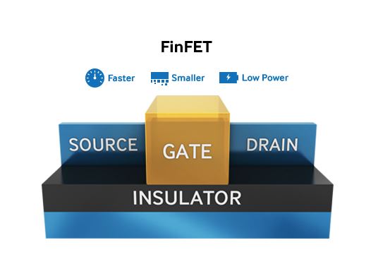
Samsung is also adding 11nm LPP (Low Power Plus) process technology to its war chest, with the new chips geared for mid- and high-end smartphones. Samsung already uses the 10nm node for its leading smartphones, such as the Galaxy Note 8, and it appears 10nm will soldier on for high-performance mobile applications. Samsung claims the 11nm LPP process boosts performance by 15% and reduces chip area by 10% (relative to 14nm LPP), which should equate to a nice power savings in tandem with the boosted performance. Samsung plans to begin 11nm LPP production in the first half of 2018.
Samsung is holding its Foundry Forum Japan event on September 15, 2017 in Tokyo. We expect more details to come to light at the event.
Get Tom's Hardware's best news and in-depth reviews, straight to your inbox.

Paul Alcorn is the Editor-in-Chief for Tom's Hardware US. He also writes news and reviews on CPUs, storage, and enterprise hardware.
-
cryoburner ReplySamsung plans to begin 11nm LPP production in the first half of 2017.
Is that so... : 3 -
Ilya__ Reply20162803 said:Samsung plans to begin 11nm LPP production in the first half of 2017.
Is that so... : 3
News article submitted via Internet Explorer? -
JTWrenn I just want a cheap, LARGE, and slow compared to other ssds but way faster than an HD storage drive already. Tired of faster faster faster, when we don't have the size.Reply -
ccampy We do have the size 2 TB ssds are allready easy to getReply
The worldwide nand shortage is what is currently holding prices up -
JTWrenn $500 for 2tb is not what I am talking about. Give me a $250 2tb that is 400MB/s and you have something. I just want them to have one system like that instead they just push one type of tech/form factor. I would much rather have old cheap chips all in one large drive at this point. Sorry but 2tb isn't going to cut it anymore.Reply
