UltraRAM Breakthrough Brings New Memory and Storage Tech to Silicon
Claims DRAM-like speeds and non-volatility for a thousand years.
Scientists from the Physics and Engineering Department of the UK's Lancaster University have published a paper detailing a breakthrough in the mass production of UltraRAM. Researchers have pondered over this novel memory type for several years due to its highly attractive qualities, and the latest breakthrough means that mass production on silicon wafers could be within sight. UltraRAM is described as a memory technology which "combines the non-volatility of a data storage memory, like flash, with the speed, energy-efficiency, and endurance of a working memory, like DRAM."

Importantly, UltraRAM on silicon could be the universal memory type that will one day cater to all the memory needs (both RAM and storage) of PCs and devices. However, we have already seen some similarly heralded ideas fall by the wayside; resistive RAM, magnetoresistive RAM, and phase-change memory, haven't made the impact that some initial reports foresaw. Moreover, we have seen Intel's Optane memory tech filling a gap between DRAM and storage but not completely bridging the divide. Intel withdrew Optane solutions for desktop PCs this time last year.
The fundamental science behind UltraRAM is that it uses the unique properties of compound semiconductors, commonly used in photonic devices such as LEDs, lasers, and infrared detectors can now be mass-produced on silicon. The researchers claim that the latest incarnation on silicon outperforms the technology as tested on Gallium Arsenide semiconductor wafers.

Some extrapolated numbers for UltraRAM are that it will offer "data storage times of at least 1,000 years," and its fast switching speed and program-erase cycling endurance is "one hundred to one thousand times better than flash." Add these qualities to the DRAM-like speed, energy efficiency, and endurance, and this novel memory type sounds hard for tech companies to ignore.
If you read between the lines above, you can see that UltraRAM is envisioned to break the divide between RAM and storage. So, in theory, you could use it as a one-shot solution to fill these currently separate requirements. In a PC system, that would mean you would get a chunk of UltraRAM, say 2TB, and that would cover both your RAM and storage needs.
The shift, if it lives up to its potential, would be a great way to push forward with the popular trend towards in-memory processing. After all, your storage would be your memory – with UltraRAM; it is the same silicon. As one use case sees success, it wouldn't be surprising to see UltraRAM deployment spread to cover from servers to PCs, to smart devices, consoles, and so on. Whether the new memory tech would be fast enough to elbow specialist fast memory types aside, like contemporary GDDR and HBM technologies, remains to be seen.
UltraRAM pricing might be another thorny issue. If it isn't price-competitive, its potential adoption rate, and transformative power, will be hindered. This economic factor remains to be seen, but the researchers were happy with the headlining silicon mass-production breakthrough of UltraRAM to make it accessible.
Get Tom's Hardware's best news and in-depth reviews, straight to your inbox.
The Lancaster University researchers say that further work is ongoing to improve quality, fine-tune the fabrication process, and implement and scale UltraRAM devices.

Mark Tyson is a news editor at Tom's Hardware. He enjoys covering the full breadth of PC tech; from business and semiconductor design to products approaching the edge of reason.
-
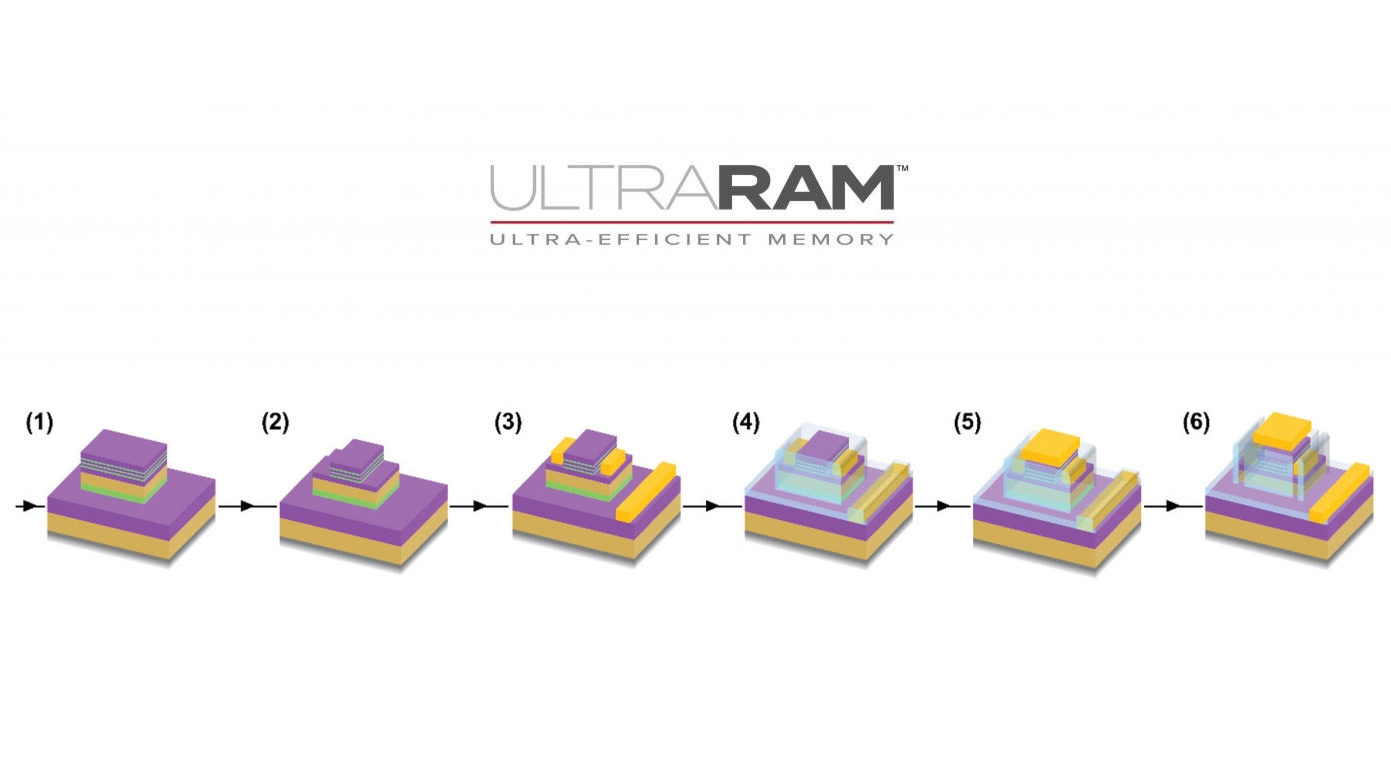
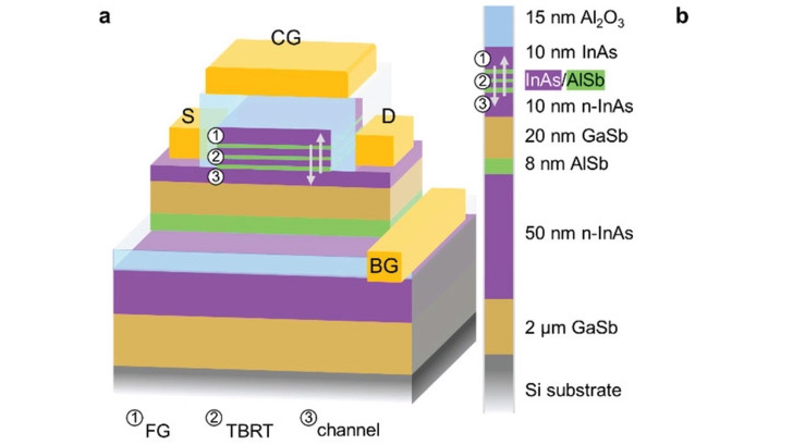
tennis2 I'm not well-versed on silicon manufacture, but that layout "stack" photo looks pretty complex and has me questioning whether that would be feasible cost effective. Not sure how this compares to a similar diagram of the stacked NAND used in SSDs. The UltraRAM stack has soooo many different elements, shapes, sizes, and locations comparatively. Not just a repeatable stack like 3d vNANDReply -
Alvar "Miles" Udell Mobile phones and tablets would be the first real benefits of this technology, assuming it's price competitive, since they don't depend on GDDR or HBM. We could finally see the end of 4GB models running Android, which is on the edge of usability now, and the speed would be perfect for advanced 4K and 8K recording, and perhaps finally move up the base specs to larger than 128GB, which is becoming a less attractive option given how the MicroSD slot is being removed on more devices. Other devices like ATMs, POS terminals, and set top boxes would also see a benefit.Reply
Outside of these markets, and perhaps specialized systems for datacenters where the cost savings of having a unified block of memory for RAM and storage, again assuming its price competitive, would bring an advantage, along with its non-volatile nature which would help minimize data loss in the event of an unexpected power loss, I have a hard time seeing it making inroads quickly.
Although I can also see AMD and nVidia using it on their professional series GPUs in the same vein as the Radeon Pro SSG to complement the on board GDDR or HBM. -
timberland67 Unless it's faster than DDR it will never be adopted for desktop/laptops as an all in one solution. Nobody wants to degrade their RAM speed just to combine the two. They should instead focus the technology to be used to make faster SSD's.Reply -
Findecanor Tech compared:Reply
Phase-change RAM:10**8 erase/write cyclesTemperature-sensitiveUltraRAM:10**7 erase/write-cycles3D crosspoint10**7 erase/write-cyclesMRAM10**8 erase/write cyclesDegrades with reading. Error rates increase with writing speed.FeRAM10**10 read/write cyclesReads are destructive, so a cell would need to be rewritten after every readNAND Flash:1000 erase cyclesMemristor
Only theoretical ("vaporware")It has sometimes been said that to be comparable to DRAM in endurance, a NVRAM technology would need to support 10**12 erase/write cycles.
I read a bunch of research papers on OS/software using NVRAM not too long ago, and it was clear that some issues still need to be resolved before NVRAM can be used as RAM:
• NVRAM still needs error detection and correction ... like on a SSD.
• NVRAM systems still need to do over-provisioning and wear-levelling ... like an SSD
• Direct access to fast NVRAM could allow malware to wear out individual cells in short time. Writes must therefore be controlled at a manageable rate.
• Read-destructive types of NVRAM still needs to be cached in DRAM
• When NVRAM is mapped into an address space, there needs to be protection against bugs in the kernel/drivers from "scribbling" into NVRAM. -
Krotow No doubt that mentioned memory type will found use in embedded devices and very fast storage devices. About using it in desktops... the next thing we want is non-volatile system memory where viruses and other malicious code can survive rebooting and power cycles.Reply