EUV
Latest about EUV
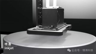
China-based firm delivers its first chipmaking tool that stamps nanoscale chip designs onto wafers
By Anton Shilov published
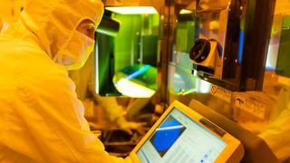
Micron samples ground-breaking EUV-based memory
By Anton Shilov published
And also a 30% increase in density
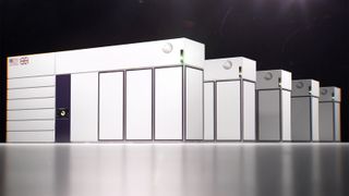
Company proposes 'tabletop' particle accelerators with petawatt lasers
By Anton Shilov published
News Analysis Y-Combinator-backed startup eyes powerful laser wakefield accelerator for advanced lithography techniques.
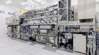
Intel has championed High-NA EUV chipmaking tools, but costs and other limitations could delay industry-wide adoption: Report
By Anton Shilov published
Delay, but not stop.
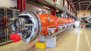
Pat Gelsinger turns to particle accelerators for a new way to make chips, joins xLight
By Anton Shilov published
Pat Gelsinger is back in the semiconductor game with xLight, a company that plans to make an EUV light source using a collider.
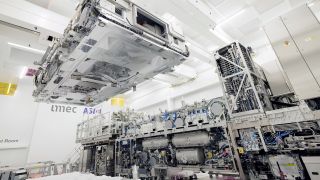
ASML teams up with Imec for sub-2nm process technologies with High-NA EUV chipmaking tools
By Anton Shilov published
ASML to install its High-NA EUV lithography tools in Imec's pilot production line to give research and development personnel access to leading-edge equipment.

Micron unveils DDR5-9200 memory: 1γ process technology with EUV
By Anton Shilov published
Micron's 1γ fabrication technology with EUV, new HKMG, and BEOL promises to increase performance while cutting power consumption for DRAM.
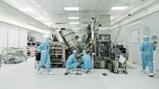
Intel has processed 30,000 wafers with High-NA EUV chipmaking tool
By Anton Shilov published
Intel says ASML's High-NA EUV tools have produced 30,000 wafers in a single quarter.
Get Tom's Hardware's best news and in-depth reviews, straight to your inbox.
