Latest about EUV

Shanghai Microelectronics Equipment patents key components of an EUV lithography tool.
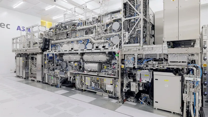
TSMC to start installing High-NA EUV system for R&D purposes this month.
Intel and Japan's National Institute of Advanced Industrial Science and Technology to establish semiconductor R&D center to advance Japanese chip industry.

SK hynix says adopting 4F2 structures and 3D transistors will increase the cost-efficiency of EUV lithography usage in DRAM production.

Samsung will be about a year behind Intel in installing ASML's Twinscan EXE:5000 High-NA litho tool for development purposes.
OIST's simplified EUV litho system uses two mirrors instead of six.

The U.S. government approves shipments of wafer fab equipment to many Chinese fabs, other are banned. Question is, can those tools be installed in banned fabs?

Tokyo Electron unveils the Acrevia tool, which can improve patterning with gas cluster beam technology.

Micron reiterates its plans to use EUV for high-volume DRAM production next year as it starts pilot production on a 1-gamma node.

Intel CEO Pat Gelsinger told Tom's Hardware during a question and answer session at Computex 2024 that China must make its own processors if US sanctions on the latest chips become too restrictive.