Latest about Manufacturing
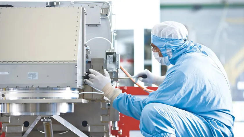
Premium ASML, Intel, Samsung, and TSMC back development of 6×12-inch to build large processors using High-NA EUV lithography systems without stitching.
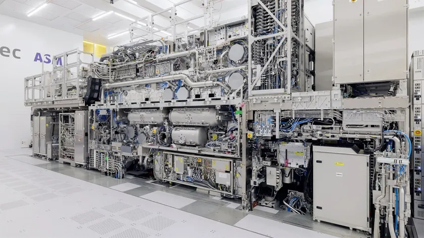
TSMC discloses plans to use High-NA EUV lithography in 2030, 6×12-inch photomasks with new scanners in 2033.
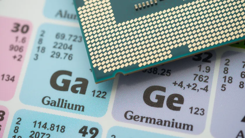
Linked Chinese company was established months after the suspect joined BelGaN
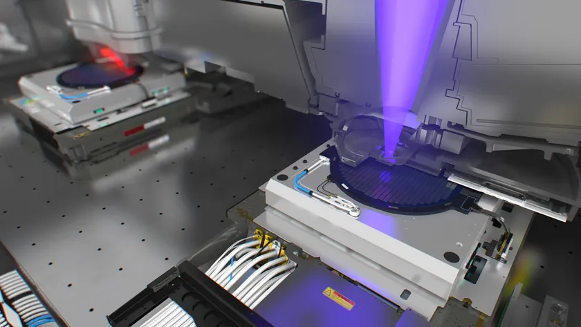
Intel is leading the semiconductor industry with High-NA fleet and process-maturity milestone as it reaches 1 million wafers processed using High-NA tools, moves forward with 6×12 photomask effort.

TSMC's equipment requirements have nearly doubled in just eight months as AI demand drives an unprecedented fab expansion, yet its 2026 CapEx budget has risen by only around 15%.
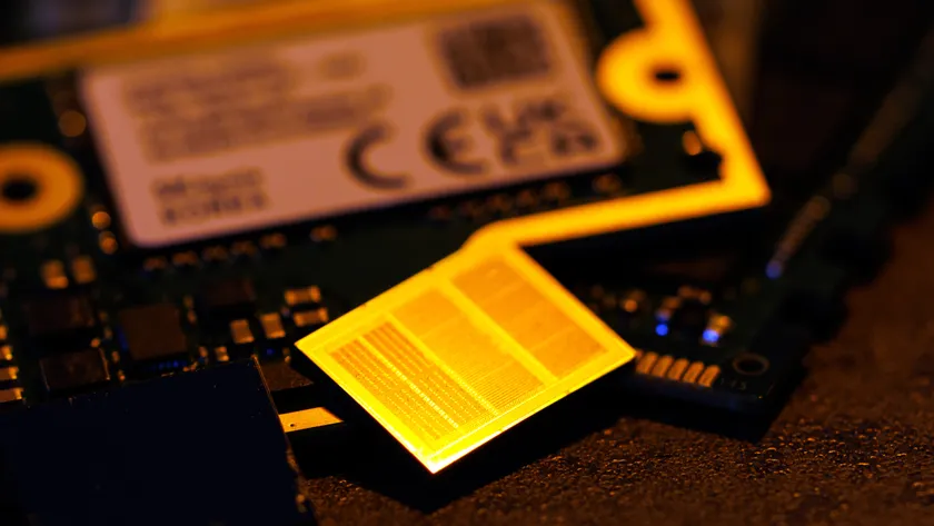
Premium Hybrid bonding, the copper-to-copper joining technique that replaces solder microbumps in 3D chip stacks, is in high-volume production on logic and freshly postponed on memory.
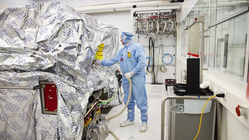
Despite rumors, there is no evidence that Chinese makers of lithography tools can produce immersion lithography scanners in quantity.

Premium Samsung detailed a three-phase HBM roadmap at Hot Chips 2026 that progressively moves logic into the base die and ultimately stacks DRAM directly on the processor.