The Ultimate Phison E7 Prototype NVMe SSDs
Introduction
Today we look into the future! It's not a crystal ball or a Ouija board, but we have parts straight from Phison's skunkworks-like project lab that are normally in stealth mode before they emerge as retail products. The double-DDR model should come to market this year, and several companies have already discussed it at CES. The real star of this show is the most aggressive emulated SLC prototype we've ever seen. They say SLC is dead, but long live low-latency single-level cell NAND, even if it's MLC programmed in SLC mode.
The double-DDR model increases the amount of DRAM the SSD uses to cache the flash translation layer map, which isn't a new trick for Phison and its partners. The Corsair Neutron XTi was the first retail product (that we know of) to use a double dose of DRAM. The XTi paved the way by increasing small-block random performance, which is the one area Phison-based SSDs need to improve to compete with Samsung on the performance front.
Phison also has a very aggressive product in its labs that we managed to escape with, and while it's more exciting, it isn’t practical in this age of low-cost consumer SSDs. Phison packed the Ultimate Phison E7 model with 1024GB of Toshiba MLC, but the flash runs entirely in SLC mode. That leaves 512GB of capacity, which Phison reduced further to 480GB due to the standard 7% overprovisioning. That means that Phison either reserves or ignores more than 50% of the flash, all in the name of performance.
Article continues belowIn my opinion, only the double-DDR model will come to market. As we mentioned, companies have already publicly discussed products based on the design. Patriot seems to be the most interested and has shown a few add-in card prototypes with different heatsinks. At Flash Memory Summit, we saw a few designs teed up as final renderings, and both look amazing. I expect to hear an announcement in March or June, but we don't have any hard evidence of a launch date.
If we do see a Phison MLC programmed-to-SLC product, it may come with Toshiba BiCS (3D) flash because Toshiba's 128Gbit 15nm MLC is too expensive. It simply takes too many die, and a high number of die per package, to build. For perspective, the SLC drive uses twice the number of 15nm MLC die compared to the double-DDR prototype reference design. The cost would nearly double for the same 480GB of user-addressable storage capacity. That doesn't mean we won't see this configuration; it's just unlikely to ship in the form we have in for testing.
Technical Specifications
| Products | The Double DDR | The Ultimate E7 SLC |
|---|---|---|
| Controller | Phison PS5007-E7 | Phison PS5007-E7 |
| DRAM | 1024 MB Nanya DDR3 | 1024 MB Nanya DDR3 |
| NAND | Toshiba 15nm MLC | Toshiba 15nm MLC w/ SLC Programming |
| NAND CapacityUser / Raw | 480GB / 512GB | 480GB / 1024GB |
| Prospects | Likely | Not Likely |
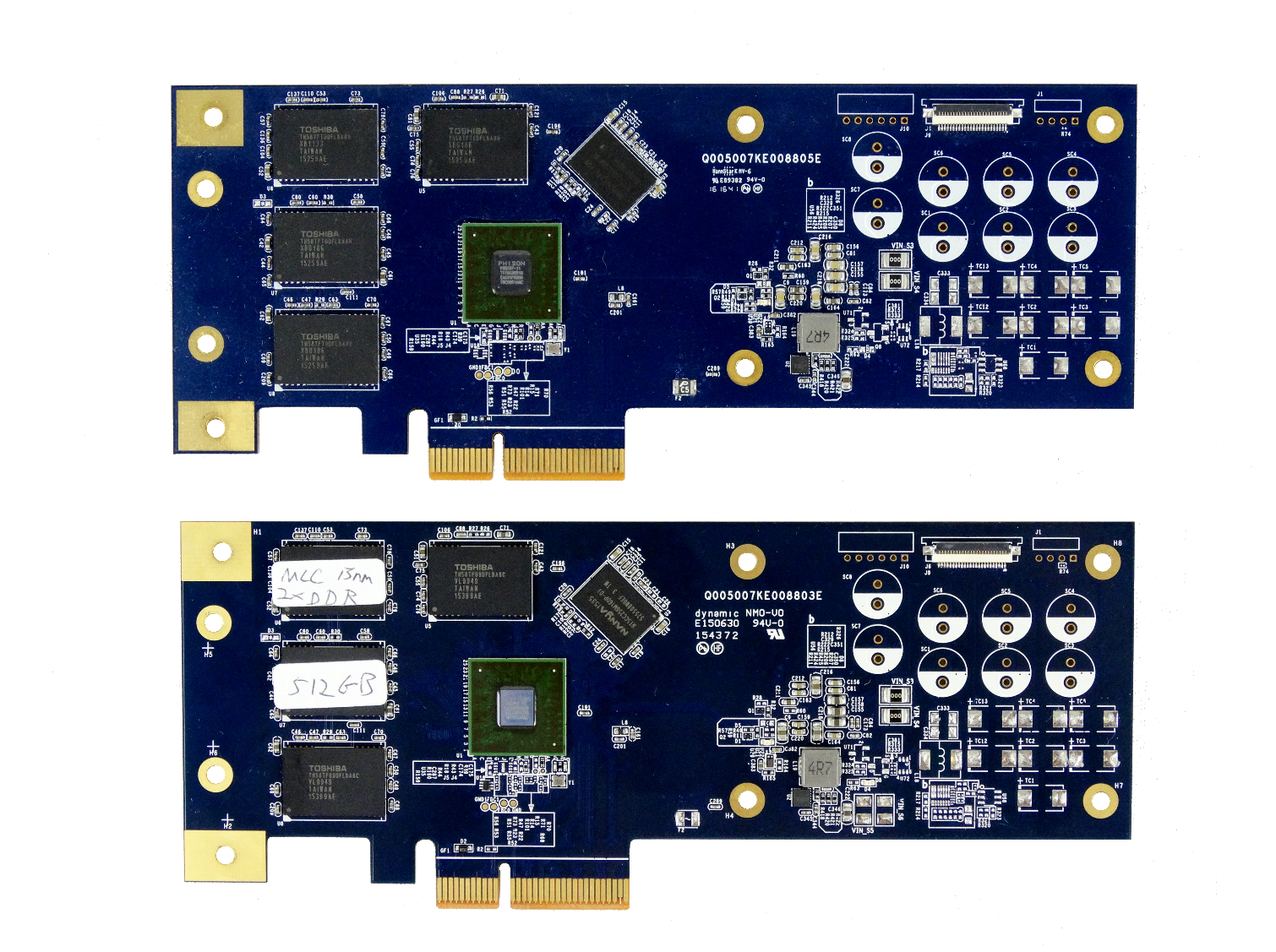
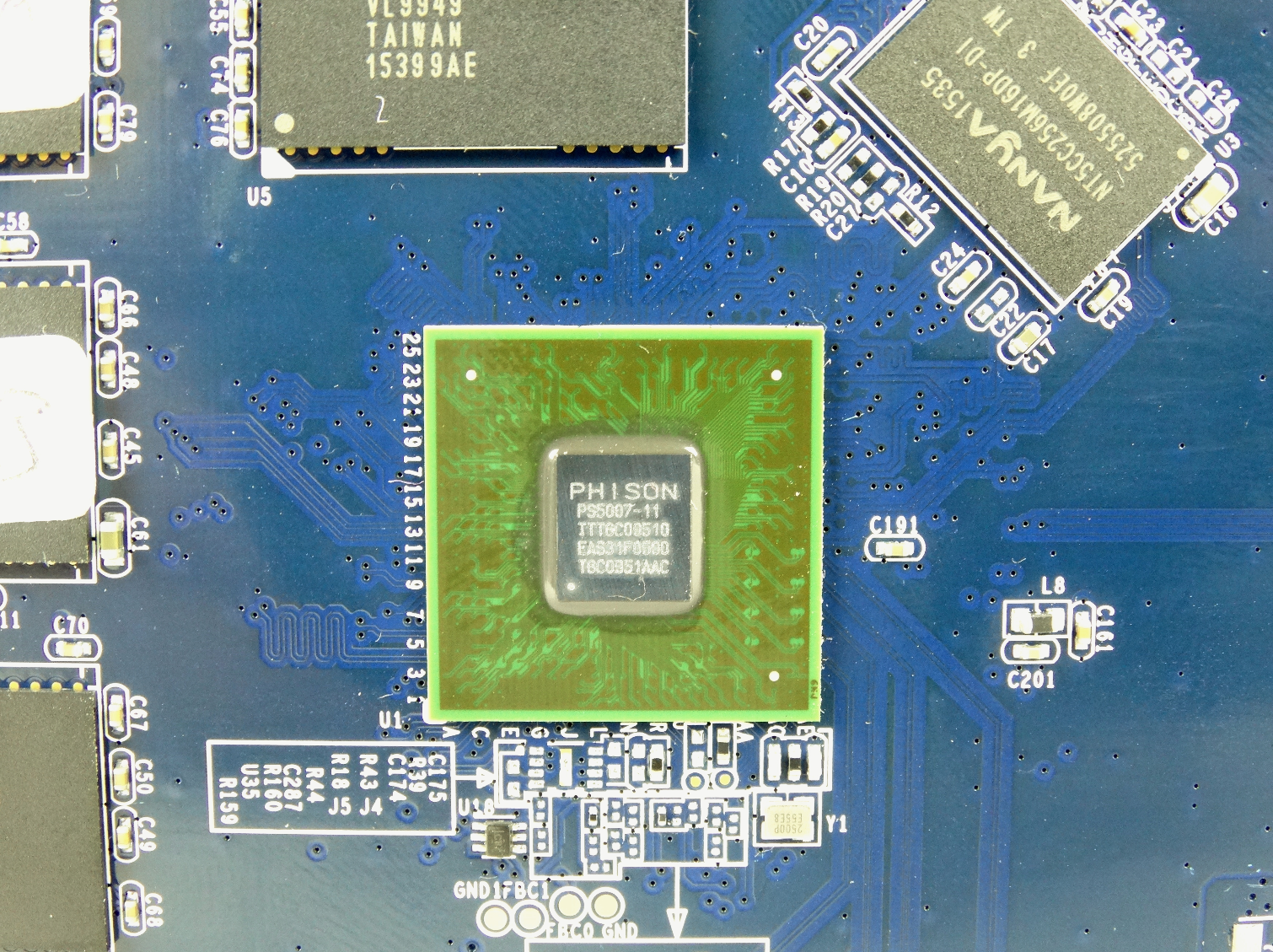
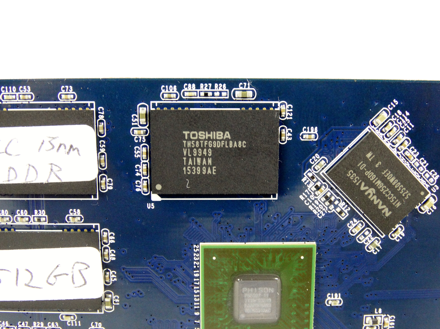
The hardware specifications of the two drives are nearly identical. Both prototype reference designs use the same Phison PS5007-E7 controller and 1024MB of Nanya DDR3 split between two 512MB packages. The drives also use Toshiba 15nm planar MLC NAND flash. The difference comes in the amount of flash; one uses a standard 512GB split between eight packages and with a usable capacity of 480GB. The SLC programming requires twice the number of raw cells to reach the same 480GB. Flash is the most expensive component on an SSD, so if Phison produces the Ultimate E7 SLC (my unofficial product name), it would cost as much as a 1TB NVMe SSD because it uses roughly the same amount of flash.
Phison didn't supply us with performance data, and it doesn’t sell prototype hardware. You won't find these drives on eBay, either. I do want to talk a little about endurance, though. The Ultimate E7 SLC NVMe SSD with two-for-one bit programming should deliver an extremely high write endurance rating that would extend beyond a regular 1TB SSD rating because of the reduced wear. Each cell only needs to decode a simple 0 or 1 value instead of MLC’s 0, 1, 2, and 3 values. The simplified process also reduces latency.
Get Tom's Hardware's best news and in-depth reviews, straight to your inbox.
As we explained in the Corsair Neutron XTi review, increasing the amount of DRAM available to the controller increases the amount of the LBA map data it can hold in high-speed DRAM. The SSD looks up data addresses on the map during read operations, and it updates the LBA map every time it writes new data. When the SSD caches the map in DRAM, the lookups and updates happen much faster, which boosts performance.
Both of our two prototype add-in cards use firmware that is at least six months old. Phison built and programmed the drives before the mass production 2.1 firmware that we first tested on the Patriot Hellfire M.2 240GB and MyDigitalSSD BPX.
Let's take a look at the drives.
A Closer Look

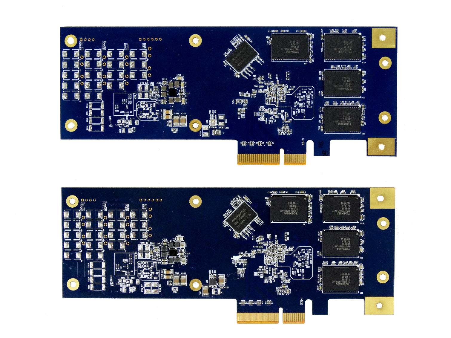
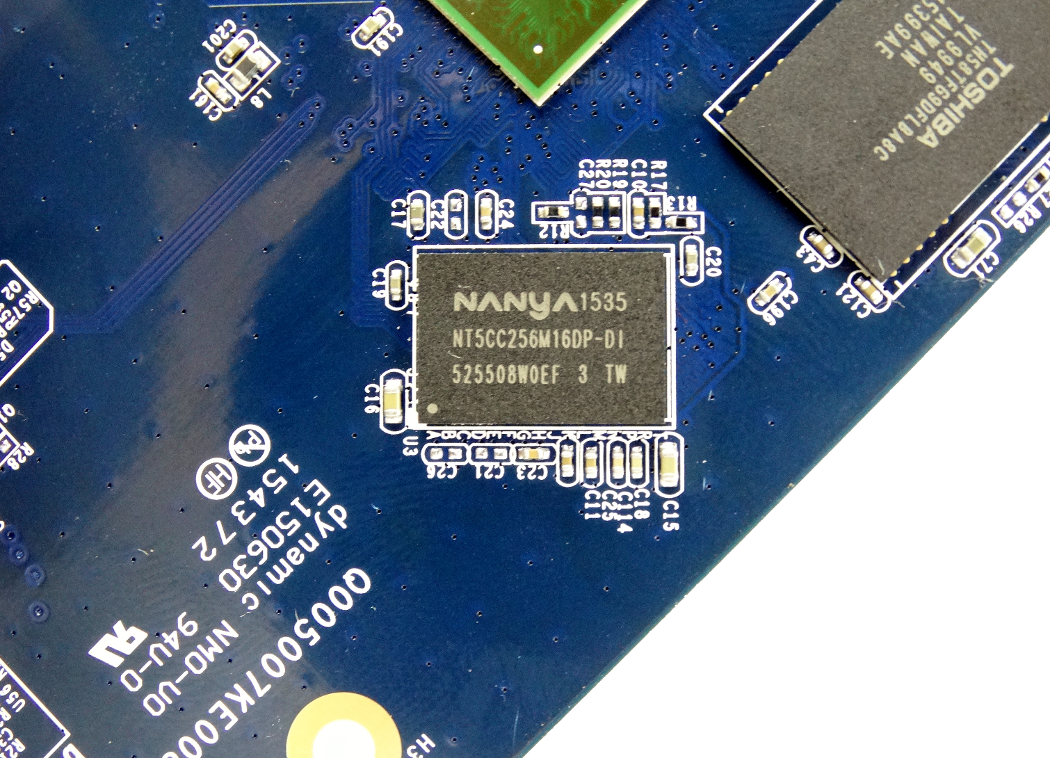
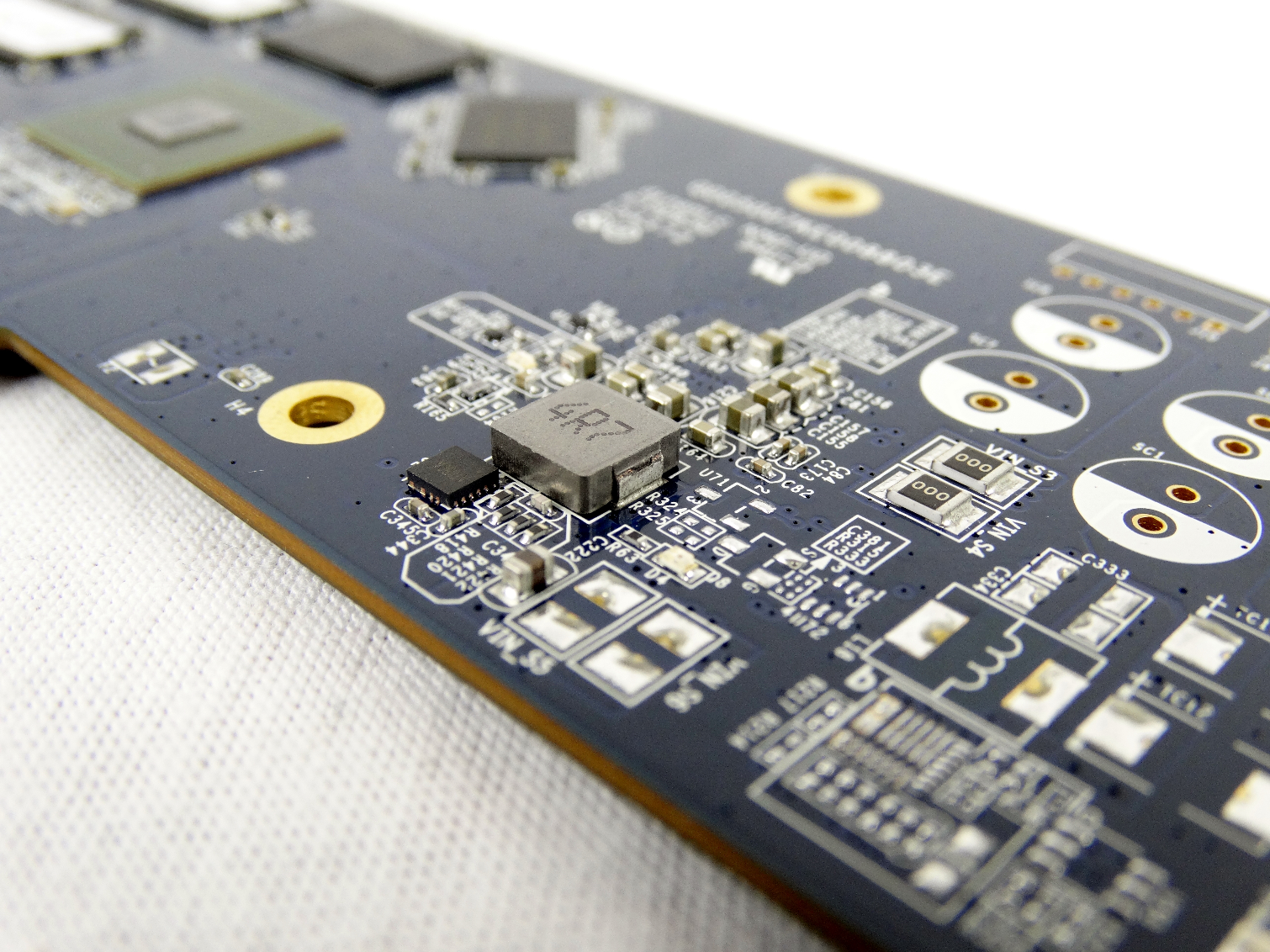
The two parts are nearly identical other than the number of NAND die in each package. The Phison add-in card reference design has several features that the company didn’t enable on either card. We'll look at the Galax Hall of Fame PCI-E SSD soon, which has some of the surface mount component pads filled with capacitors for advanced host-power failure features. Our prototype reference design parts don't have those features enabled because they aren't meant to operate in a production environment.
MORE: Best SSDs
MORE: How We Test HDDs And SSDs
MORE: All SSD Content

Chris Ramseyer was a senior contributing editor for Tom's Hardware. He tested and reviewed consumer storage.
-
kalmquist If it were purely a matter of cost of materials, one might expect a 240 GB SLC drive to cost the same as a 480 GB MLC drive. That would probably get some customers looking to combine a fast boot drive with a slower drive for mass storage, but not necessarily enough to cover the engineering and validation costs.Reply -
jchang6 An SLC device priced the same as 2X capacity MLC would definitely be interesting, more so if it could be programmed by the userReply -
drajitsh It is speculated that Samsung Z-nand could be 3d-SLC. With a large memory buffer (with power loss caps, of course), a specially made for SLC controller, and a SLC specific firmware it could challenge intel x point.Reply -
lsorense Using the flash in pseudo SLC mode does not mean ignoring half the flash. It also does not mean using twice as many cells to store things. What it does mean is that instead of storing 2 bits per cell as MLC does, you store 1 bit instead, by not using the two middle voltage levels. So if MLC mode stored 00, 01, 10, and 11 using the voltages 0, 0.5, 1.0 and 1.5 (I am sure these are not the right ones, but it's the idea), pseudo SLC mode would just store 0 and 1 using 0 and 1.5 volt. This has the advantage for reliability that you can treat any cell with a value of between 0 and 0.6 as a 0 and any value between 0.9 and 1.5V as a 1, which is much more tolerant of cell wear than MLC mode where you have to be more in the range of 0 to 0.2V, 0.4 to 0.7V, etc. Since it has much more tolerance, it can stay working much longer than in MLC mode. Whether using it in pseudo SLC mode makes it any faster than MLC I don't know. I don't actually see why it should, but perhaps reading and writing the middle voltage levels is slower than just the top and bottom.Reply
