GlobalFoundries Expands Production Capacity With a $4 Billion Fab in Singapore
GlobalFoundries expands production capacities in Singapore.

GlobalFoundries this week started construction of a brand new fab in Singapore in a bid to expand the supply of chips made using its speciality process technologies. The company and its partners will co-invest $4 billion in the new production facility that will start ramping up production in 2023.
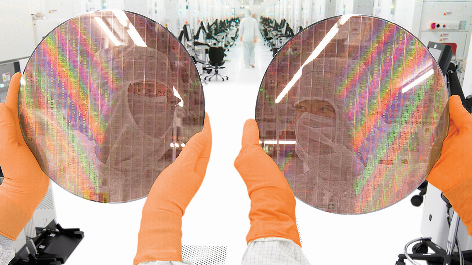
The new Fab will feature 250,000 square feet (23,000 square meters) of cleanroom space and will process around 450,000, 300-mm wafers per year (approximately 37.5 thousands wafer starts per month) using a variety of technologies, such as those used to build RF, analog power, non-volatile memory solutions. The new fab will employ over 1,000 of engineers and technicians. When the fab is completed, the whole GlobalFoundries campus in Singapore will process over 1.5 million 300-mm wafers per year.
Being one of the world's largest speciality contract makers of semiconductors, GlobalFoundries is in process of expanding all its production capacities in order to meet growing demand for its services. This year the company also plans to invest in new manufacturing tools to increase production of its Fab 1 in Dresden, Germany, and Fab 8 in Malta, New York.
The new fab will cost over $4 billion, which will be co-invested by GlobalFoundries, the Singapore Economic Development Board and committed customers. GlobalFoundries says that the new semiconductor production facility will be the most advanced in Singapore, which is not particularly surprising since no foundry has built a new leading-edge fab in the country for about a decade since GlobalFoundries bought Chartered Semiconductor in late 2009.
GlobalFoundries is getting ready for an IPO in late 2021. Before going public, the company has to make its plans clear to potential investors and starting to build a new fab and investing in additional tools for existing facilities is a way to show the direction of management. Also, increasing production is a message to GlobalFoundries' existing customers that the company will do everything it can to meet their demand in the future.
"GF is meeting the challenge of the global semiconductor shortage by accelerating our investments around the world,"said GF CEO Tom Caulfield. "Working in close collaboration with our customers and the Government of Singapore is a recipe for success that we are pioneering here and looking forward to replicating in the U.S and Europe. Our new facility in Singapore will support fast-growing end-markets in the automotive, 5G mobility and secure device segments with long-term customer agreements already in place."
Get Tom's Hardware's best news and in-depth reviews, straight to your inbox.

Anton Shilov is a contributing writer at Tom’s Hardware. Over the past couple of decades, he has covered everything from CPUs and GPUs to supercomputers and from modern process technologies and latest fab tools to high-tech industry trends.
-
InvalidError TSMC GloFo having to invest 4G$ in what likely is a new 14nm-class fab shows that demand for chips made on older processes is still alive and well despite popular belief that chip manufacturers who aren't investing in bleeding-edge processes are doomed. Support chips made on 22-1200nm processes may not be making headlines anymore but they are still very much needed today.Reply -
InvalidError Reply
Oops :)mamasan2000 said:GloFo, not TSMC
Well, that makes an even stronger case about the market for ~14nm processes being alive and well. -
AgentLozen I haven't heard anything about Global Foundries in a long time. I'm glad that they're alive and well. Thriving even, it seems.Reply
They were making 12nm chips for AMD a few years ago then they announced that they weren't planning to move to 7nm. Does anyone know if they're still making 12nm chips? -
InvalidError Reply
A 7nm fab costs ~10G$ to build, so I think we can say with pretty high confidence that 4G$ must be 14nm-class.AgentLozen said:Does anyone know if they're still making 12nm chips?
The fab is earmarked primarily for analog, RF and power management stuff which doesn't need bleeding-edge process tech: analog stuff requires bulky relatively high current components and traces, RF requires relatively large planar passive components along with possibly significant power and power management stuff requires large transistors, all stuff that does not benefit much from process shrinks except for tighter tolerances, higher yields.
Using a 14nm-class process to make parts that would likely be perfectly fine on 45+nm does have the benefit of opening the option to make stuff down to ~14nm should the need arise.
As I have written in previous threads about GloFo's "imminent" demise, everyone will need someone to make interposers and substrates of all sorts when all major chips go with some version of 3D-stacking and 12-22nm will also be perfectly fine for that. It may not be as glorious as making the bleeding-edge parts of future chips but it should keep GloFo afloat for the next 10+ years. -
hotaru.hino Reply
And even then, there's still a ton of demand and use for 8-bit, 16-bit, and stupid simple 32-bit micros. When those things are literally a buck or two, it doesn't really make much sense to spend 10 figures on something that needs an astronomical amount of volume to recoup the cost.InvalidError said:As I have written in previous threads about GloFo's "imminent" demise, everyone will need someone to make interposers and substrates of all sorts when all major chips go with some version of 3D-stacking and 12-22nm will also be perfectly fine for that. It may not be as glorious as making the bleeding-edge parts of future chips but it should keep GloFo afloat for the next 10+ years.