How SSDs Work
With the internal SSDs we're discussing today, flash memory and a controller are installed onto a printed circuit board (PCB) and packaged into a small enclosure. This housing is typically in one of the 1.8”, 2.5”, or 3.5” form factors that we all know and love from conventional hard drives. These can be mounted into PCs, laptops, or certain rackmount server environments. Indeed, flash SSDs look and largely behave like hard drives, with the exceptions that there are no moving parts and they weigh less. In addition, modern SSDs require very little cooling. Most SSDs employ a 2.5” housing and utilize 3 or 6Gb/s interface speeds.
MLC and SLC NAND Flash
Internally, all flash SSD products store data onto either single-layer cell (SLC) or multi-layer cell (MLC) NAND memory, able to store a single bit or multiple bits per cell, respectively. SLC cells offer less capacity per transistor than MLC, but higher write performance and data durability.
Modern Controller Architectures
All SSD designs are based on flash controllers that drive the storage circuits and connect to the host system via Serial ATA. Modern designs utilize the controller "brain" to tackle various needs. For example, data durability is addressed through wear leveling algorithms, ensuring that flash memory cell usage distribution is as even as possible to maximize the device’s life span. Performance is optimized through multiple flash memory channels, load balancing, and different methods of caching. Some controllers have an integrated cache, others work with a separate DRAM memory chip, and other designs utilize a part of the flash memory across multiple channels for data reorganization. Please read the article Tom’s Hardware’s Summer Guide: 17 SSDs Rounded Up for more details on architectures and specific products.


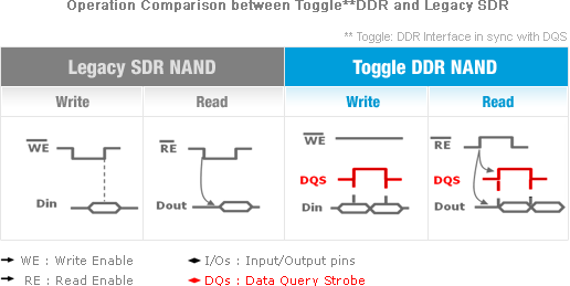
Trend: Toggle DDR NAND Flash
Samsung introduced Toggle DDR NAND flash memory a few months ago. This is a flash memory design that transfers data during the rising and falling edge of a memory signal, much like DDR DRAM. This approach debuted in the enterprise segment but will soon also be available in consumer SSDs. The main benefit of Toggle DDR is its increased bandwidth of 66 to 133 Mb/s per channel as opposed to 40 Mb/s. Drives using the new approach will probably not employ the faster peak bandwidth, but will instead try to maximize SATA II performance on 3 Gb/s interfaces while further lowering power consumption. We’ll explain in a bit why this is important.