Phenom vs. Athlon Core Scaling Compared
A Quick Processor History Lesson
The Athlon 64 family had been superior to Intel's Pentium 4 or Pentium D offerings most of the time from the AMD64 launch in 2003 and Intel's introduction of the Core microarchitecture in 2006. While the Pentium 4 and Pentium D were aimed at reaching high clock speeds, their power requirements grew faster than the performance benefits. As a consequence, AMD's approach of delivering more performance per clock was clearly more successful. Intel realized that a reasonable balance between processing cores and clock speed, based on the available manufacturing technologies, provides a much better path to more performance at reasonable power requirements. This eventually helped the company to get the crown back with Core 2 Duo.
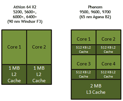
While Intel had mainly been fitting multiple units of its processors into one physical package to create multi core processors - such as the Pentium D 800 at 90 nm and Pentium D 900 at 65 nm - AMD decided to go for more integration right from the start. The first Pentium D held two Pentium 4 units on a single die, but they used the Front Side Bus to communicate. The second generation Pentium D 900 included two dies inside the physical processor. The Athlon 64 X2 dual core also consists of two Athlon 64 cores, but they are on one die, and AMD implemented a crossbar switch as well as a shared memory controller per processor. Inter-core communication hence does not tax the system interface, which is either AMD's HyperTransport or Intel's Front Side Bus.
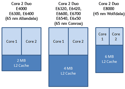
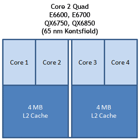
With the introduction of Core 2 Duo, Intel finally placed two processors together with a unified L2 cache onto a single die, which, among several other improvements, is the secret behind the leading performance per watt ratio of the Core 2 product line. As it makes a lot of sense to accommodate two processor dies inside a processor package to double the core count, Intel approached this strategy to create its Core 2 Quad processor. Essentially, it consists of two Core 2 dual cores and again depends on a fast Front Side Bus when one dual core has to exchange data with the other.
AMD insisted on providing a "true" quad core, which has now been made available as the Phenom processor. While Intel introduced a shared L2 cache (used by all cores) with the Core 2 Duo and pairs two of them to create a quad core unit, AMD went a step farther and added a shared 2 MB L3 cache for all, keeping 512 kB L2 cache per core. Intel's next-generation Core 2 processors, based on the 45 nm Wolfdale core, increase the L2 cache capacity by 50% (6 or 3 MB instead of 4 or 2 MB).
While AMD can control processor characteristics such as clock speed for each core in greater detail, the Agena/Barcelona quad core design is also highly dependent on reliably high manufacturing yield rates. Dysfunctional processing cores on an Agena die force AMD to sell the product as a triple or dual core, while Intel has the flexibility to take any two Core 2 dies to create its quad core units. In theory, AMD's approach offers the better quad core design, while Intel's strategy makes more sense from a business standpoint. Eventually, all we really care about is the result: do the products deliver what their makers promise?
Get Tom's Hardware's best news and in-depth reviews, straight to your inbox.
Current page: A Quick Processor History Lesson
Prev Page How Well Does Phenom Scale With Clock Speed? Next Page Athlon 64 X2 At 2.2, 2.4, 2.6 And 2.8 GHz
Patrick Schmid was the editor-in-chief for Tom's Hardware from 2005 to 2006. He wrote numerous articles on a wide range of hardware topics, including storage, CPUs, and system builds.


