Two-Die Xeon? Leaked Sapphire Rapids Photo Appears to Show Chiplets
Intel's Sapphire Rapids seems to use two dies, early photos reveal.

A member of ServeTheHome forums has published what he claims to be the first photos of Intel's Xeon Scalable 'Sapphire Rapids' processor. If the images are legitimate, they may shed some light on the design of the CPU and may indicate that it does not use a large monolithic die, but actually carries two dies.
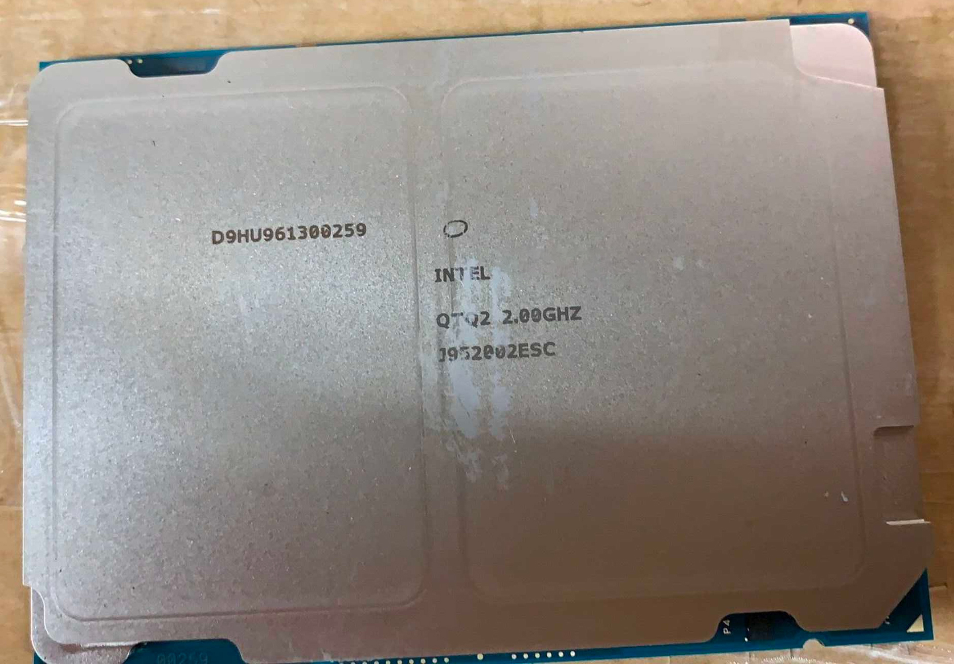
The photos depict an LGA processor with a metallic heat spreader carrying an 'Intel Confidential' mark, which indicates that this is a pre-production chip meant for testing and evaluation. Another engraving indicates a rather moderate 2.0 GHz frequency of the CPU which is something to be expected from an early sample. Also, since the processor is a pre-production sample, it has a four-character stepping: QTQ2. Since the device does not look like an existing Intel processor, it could well be a sample of Intel's upcoming Sapphire Rapids.
The front side of the alleged Sapphire Rapids processor reveals a rather intriguing detail. The heat spreader of the CPU has two bulges of about the same size. Intel's contemporary CPU heat spreaders do feature a number of convexities, but there is always one main 'bump' above the main die. Two bulges may indicate that Intel uses two processor dies for Sapphire Rapids instead of one monolithic die.
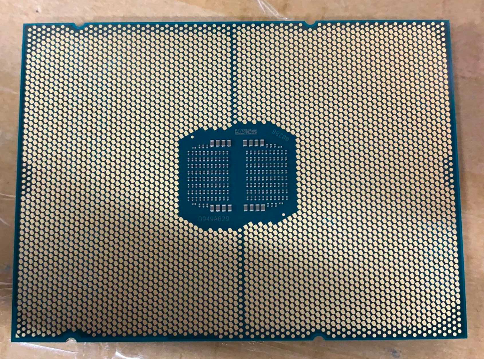
The back side of the CPU looks typical for Intel's latest server processors with its land grid array split into two domains. Meanwhile, there are two identical sets of capacitors in the middle of the package, which supports the theory that Intel's Sapphire Rapids is indeed a multi-chip-module (MCM) carrying two dies interconnected using one of Intel's latest technologies (e.g., EMIB). By contrast, Intel's monolithic dies have one set of capacitors on the back of their packaging.
Using an MCM — or chiplet — design has a number of advantages when it comes to development and manufacturing. For obvious reasons, it is easier to design, emulate, and debug smaller chips. It is also easier to hit decent clocks and yield levels with smaller dies. On the other hand, large monolithic dies work more efficiently as internal interconnections are always faster than off-chip interconnects.
As a rule, Intel does not comment on leaked information about its unreleased products, so do not expect the company to confirm or deny any facts about its Sapphire Rapids processor beyond what is has already been revealed.
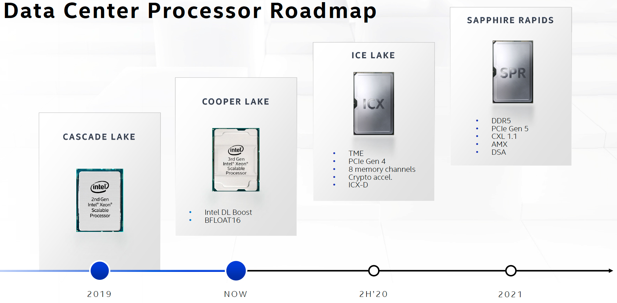
So far, Intel has publicly confirmed that its Sapphire Rapids processors will use the Golden Cove microarchitecture that supports Intel’s Advanced Matrix Extensions (AMX) as well as AVX512_BF16 and AVX512_VP2INTERSECT instructions that are particularly well suited for datacenter and supercomputer workloads.
Get Tom's Hardware's best news and in-depth reviews, straight to your inbox.
In addition to microarchitectural innovations, the new CPU will feature a DDR5 memory controller (enhanced with Intel’s Data Streaming Accelerator, DSA), the PCIe 5.0 bus with a 32 GT/s data transfer rate that is enriched with the CXL 1.1 protocol to optimize CPU-to-device (for accelerators) as well as CPU-to-memory (for memory expansion and storage devices) interconnects. Intel will produce Sapphire Rapids using its 10 nm Enhanced SuperFin technology.

Anton Shilov is a contributing writer at Tom’s Hardware. Over the past couple of decades, he has covered everything from CPUs and GPUs to supercomputers and from modern process technologies and latest fab tools to high-tech industry trends.
-
hotaru251 intel really should stop trying to put down amd since they seem to do exactly that later on.Reply -
mitch074 Reply
Yeah - it's almost becoming a meme.hotaru251 said:intel really should stop trying to put down amd since they seem to do exactly that later on.
486 - clocking it higher is expensive. AMD pulls out the DX4-120.
Pentium / K6 : Socket 7 is dead at 233 MHz. AMD pulls out the K6-III+ at up to 570 MHz officially.
Pentium III : 1 GHz and over is not stable with a short pipelined architecture. AMD pulls out the Athlon.
Pentium 4 : Rambus and high frequency is the future. AMD beats it to a pulp with Athlon XP and DDR.
Itanium : x86 can't do 64-bit properly. AMD pulls out x86-64.
Core 2 : integrated memory controller is useless. AMD enables dual channel DDR/DDR2 on consumer-level stuff (sockets s939 and AM2) - the IMC was already there on all their x86-64 chips.
Core 2 Quad up to 7th generation Core i : more than quad core is useless for daily computing. AMD pulls out six-core Phenom, and (much later, Bulldozer was a major blunder in the PC space, although it worked on consoles) Ryzen 1700.
Up until now : thread safety is a gimmick. AMD : pulls out Bulldozer for consoles.
Up until now : glued cores are bad for performance. AMD pulls out Threadripper (up to 2 dies did work quite nicely) then Zen 2-3 (up to 8 dies in a single package).What's next? BAR address range resizing is only for big businesses? ECC DDR has no use in the consumer space? Weak embedded graphics are good enough for desktop users? -
JfromNucleon As much as this is good news, I feel that Intel (and AMD for that matter but especially Intel) will eventually move back to a monolithic die.......... unless something else happens. ..............Reply -
escksu I highly doubt intel is using chiplets. What they usually do is to combine 2 dies to double the core countReply -
Neilbob Replyescksu said:I highly doubt intel is using chiplets. What they usually do is to combine 2 dies to double the core count
Yes, this.
I bet each of those 'chiplets' is about twice as large as an entire Ryzen CPU. This is probably more like the Pentium D 2021 edition. ;) -
usiname Reply
Later? More like years agohotaru251 said:intel really should stop trying to put down amd since they seem to do exactly that later on.
https://cdn.wccftech.com/wp-content/uploads/2019/12/Intel-SoMa-3.png -
nofanneeded At First I thought it was XE Graphics beside the CPU , but looking at it from behind , they looke two identical chips not CPU + GPUReply -
thGe17 Reply
In the end this doesn't matter. It is a MCM design one way or the other.escksu said:I highly doubt intel is using chiplets. What they usually do is to combine 2 dies to double the core count
Additionally this would give them the opportunity to double memory channels (and probably also PCIe lanes), if they intend to (?), as they have already done with Cascade Lake AP with 12 memory channels.
Finally it is very likely, that this design (if it's no fake) will simply be an extension to their expertise with Cascade Lake AP.
The main question is: How efficient will be their third process iteration 10nm+++ aka Enhanced SuperFin because this will limit core scaling in the end. The design will be released after Milan and most likely outperform it (in special workloads even by far), but it will be released shortly before Genoa in 5nm, which puts it in a difficult position (because originally Granite Rapids SP in 7nm should have been the competitor for Genoa, but with the 7nm delay, this server will arrive not until the first half of 2023).
Of course it will be larger. Already Ice Lake SP will provide 32 to 36 (?) cores on a monolithic die, therefore of course it is significantly larger than a Ryzen CPU with only up to 16 cores. :rolleyes:Neilbob said:Yes, this.
I bet each of those 'chiplets' is about twice as large as an entire Ryzen CPU. This is probably more like the Pentium D 2021 edition. ;)
Btw: 3900/50X and 5900/50X require ~ 273 mm2 die area.
Skylake SP (in 14nm) as HCC with up to 18 cores has about ~ 428 mm2, therefore you can estimate that an HCC for Ice Lake SP or Sapphire Rapids SP will be significantly smaller and therefore still larger but far away from doubling the area (compared to a Ryzen).
But if you had something different in mind, a 64 core Rome/Milan/Threadripper has a die area of about ~ 1008 mm2. This also means, that a 64 core Sapphire Rapids SP most likely *) will only require a few square millimeters more (if at all) than Milan, because Intel produces these die(s) completely in 10nm whereas AMD still uses a very large 14nm IO-die (the IO-die for Ryzen's is produced in 12nm, the one for Rome in 14nm; currently it is unclear if AMD had possibly shrinked it to 12nm for Milan).
A 32 core Epyc/Threadripper currently requires at least ~ 712 mm2 with four chiplets, therefore it is safe to assume, that a 32 core Intel die will require less area. Already a 28 core Skylake SP in 14nm only requires 602 mm2.
*) "Most likely" because it also depends on the amount of increased caches and possibly "much broader" cores. -
JayNor Replyescksu said:I highly doubt intel is using chiplets.
Intel presented their intentions to use smaller chiplets for what they call Client 2.0.
AMD's Norrod explained how they need to move to 3D mfg. for performance.
See his presentation video and discussion
https://www.tomshardware.com/news/amd-3d-memory-stacking-dram,38838.html
Intel and TSM both are developing hybrid bonding. Intel announced a hybrid-bonded SRAM test chip recently.
https://www.servethehome.com/intel-10nm-superfin-and-10nm-enhanced-superfin-hybrid-bonding/intel-architecture-day-2020-packaging-hybrid-bonding-on-sram-stacks/


