Kioxia Unveils Potential Successor to QLC NAND Flash
The company formerly known as Toshiba has an idea for what comes after quad-level cell NAND flash.
Kioxia (formerly Toshiba Memory) has developed a new technology to increase the storage density of flash memory called Twin BiCS Flash. The technology, announced Thursday, essentially allows memory chips to have smaller cells and more bits per cell, both of which can lead to increased memory density.
The Twin BiCS Flash is a candidate for 3D NAND flash drives with more than four bits per cell (aka QLC). The company gave us some hints about the technology for the first time at the Flash Memory Summit 2019 in August, when it presented its “halved memory cell” technology for denser 3D NAND drive. Kioxia was still called Toshiba Memory at the time.
On Thursday, Kioxia publicly announced the world’s first “three-dimensional semicircular split-gate flash memory cell structure." The Twin BiCS Flash name coincides with another technology Kioxia currently develops and manufactures with partner Western Digital, BiCS Flash.
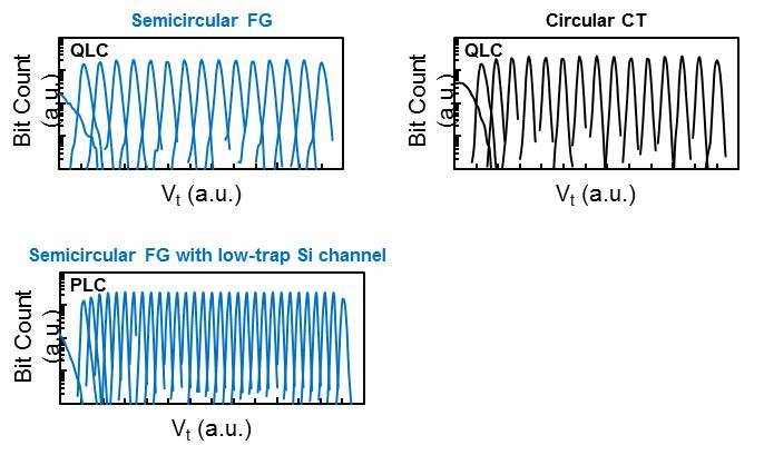
Article continues belowUnlike BiCS Flash, which uses a circular charge trap cells (CT), the new Twin BiCS Flash uses semi-circular floating gate cells (FG). The new structure enlarges the window for programming the cell, even though the cells are smaller than with CT technology. This makes the technology quite a promising candidate to succeed the QLC NAND technology, although it’s not clear yet if it will become penta-level cell (PLC) technology or something else.
Normally there are three ways to increase NAND flash density.
One is to increase the memory layers. We’ve recently passed 96-layer NAND flash chips and achieved 128-bit NAND flash chips. Manufacturers are already envisioning 500 and 800-layer NAND chips in the future.
Another is to increase the bits per cell, which has given us SLC, MLC, TLC and, more recently, QLC NAND, with each one increasing the number of bits per cell by one compared to the previous technology (usually with a trade-off in reliability).
Get Tom's Hardware's best news and in-depth reviews, straight to your inbox.
And the third is to decrease the cell size so that more cells can fit in a single layer.
Kioxia’s Twin BiCS Flash technology focuses on the latter two, as the company believes that as we pass over 100 NAND memory layers there are diminishing returns from increasing the number of layers with each generation. The trade-offs look less and less appealing compared to the other two ways to increase density, according to Kioxia.
The company said in in its announcement
"3D flash memory technology has achieved high bit density with low cost per bit by increasing the number of cell stacked layers as well as by implementing multilayer stack deposition and high aspect ratio etching. In recent years, as the number of cell layers exceeds 100, managing the trade-offs among etch profile control, size uniformity and productivity is becoming increasingly challenging. To overcome this problem, Kioxia developed a new semicircular cell design by splitting the gate electrode in the conventional circular cell to reduce cell size compared to the conventional circular cell, enabling higher-density memory at a lower number of cell layers."
Twin BiCS Flash is still years away from implementation and very much in the research and development phase.
Kioxia is now preparing its launch of BiCS5 128-layer NAND flash chips in 2020. Both SK Hynix and Samsung were able to pass the 100-layer milestone earlier this year, with the 128-layer 4D NAND and V-NAND v6, respectively.
Lucian Armasu is a Contributing Writer for Tom's Hardware US. He covers software news and the issues surrounding privacy and security.
