Tom's Hardware Visits STMicroelectronics In Rennes, France
Highly Rigorous Tests
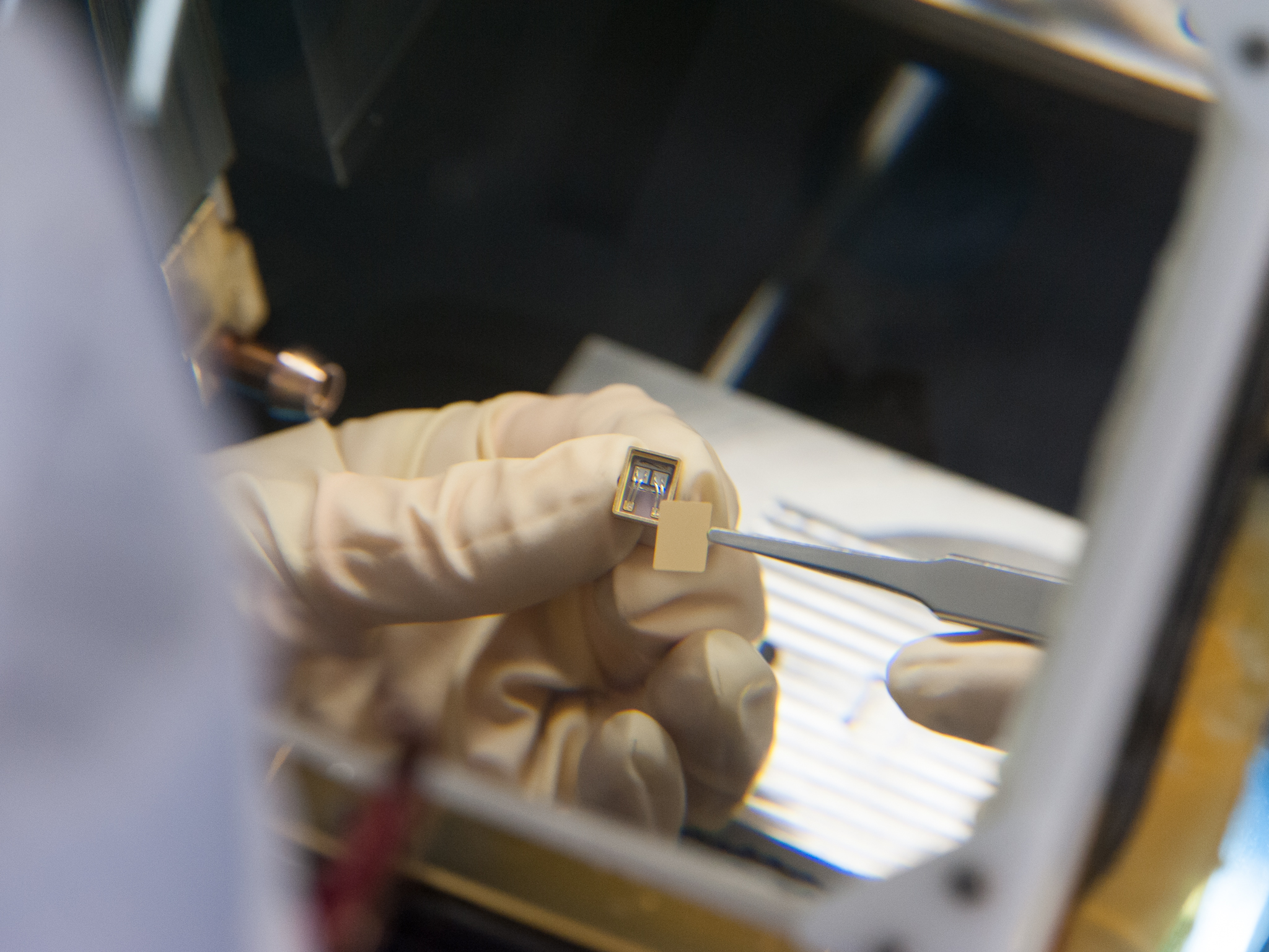
Once the die is mounted in its case, the wires must be soldered to connect the chip and the pins. This operation can seem archaic compared with the processors used in PCs or smartphones, whose dies are connected via direct contact with bumps on their epoxy carriers. But due to the reliability constraints of the aerospace sector, older, tried, and proven methods are used.
The certifications require that the wires be tested for mechanical strength. Here again, a percentage of the components will be culled from the production lines to undergo destructive tests to determine the force needed to break the wires and the failure mode (at the chip, at the case, in the middle of the wire, etc.).
The next stage is closure of the case, which must be totally hermetic. To avoid corrosion, the dies are kept in a dry nitrogen atmosphere. The case is sealed in various ways depending on its shape, size, and type. Ceramic cases are sealed in a furnace. Metal ones can be sealed using electrical welding. STMicroelectronics has 34 different cases in its catalog and needs to have that many devices available for sealing them.
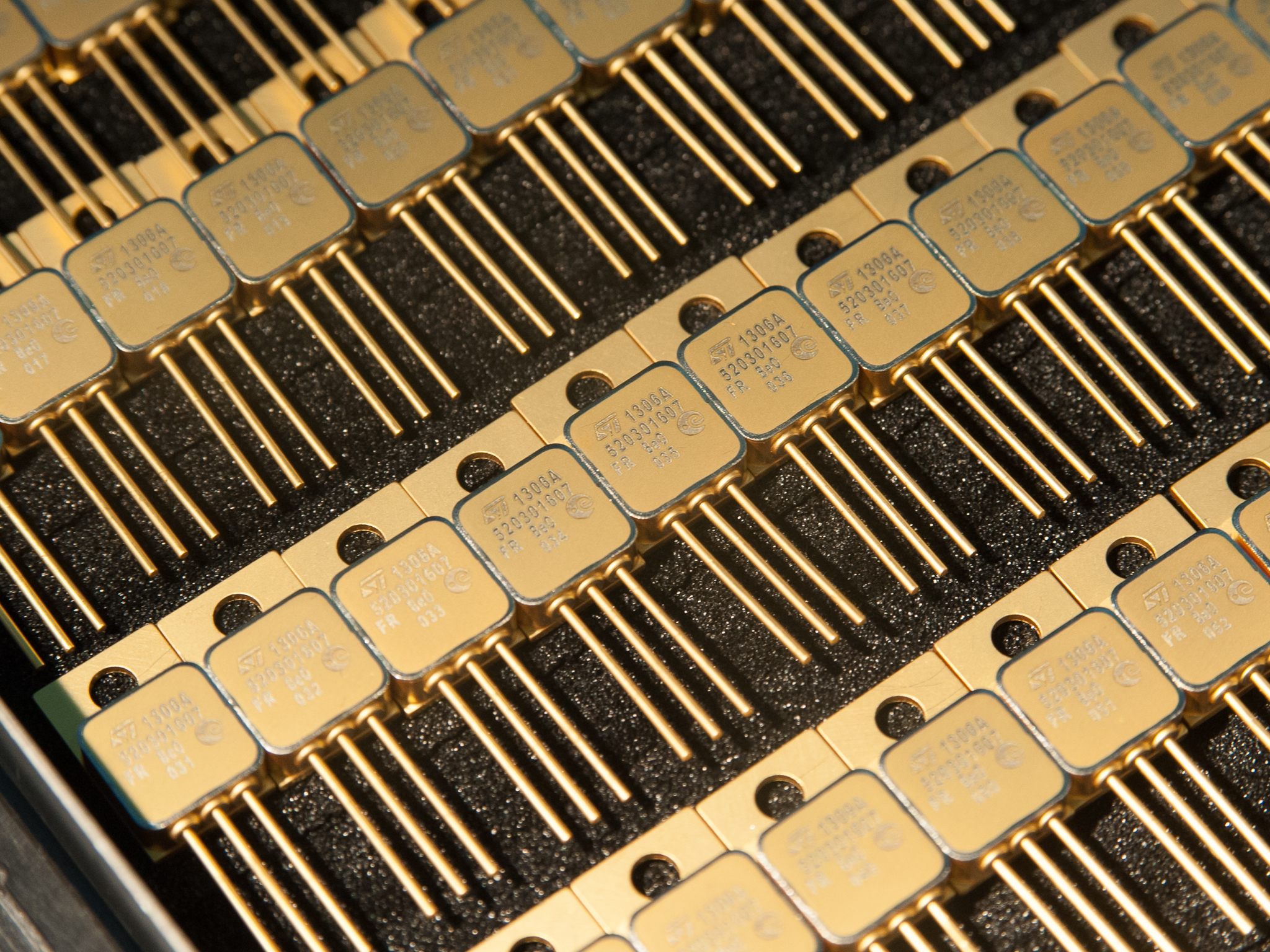
Once the case is sealed, all that remains is to mark it. STMicro Rennes recently moved from ink marking to laser marking, which is more durable. Fabrication as such is now complete. But ahead is a long period of tests to verify the quality of the fabrication and the chip’s resistance to aging.
Real Little Jewels
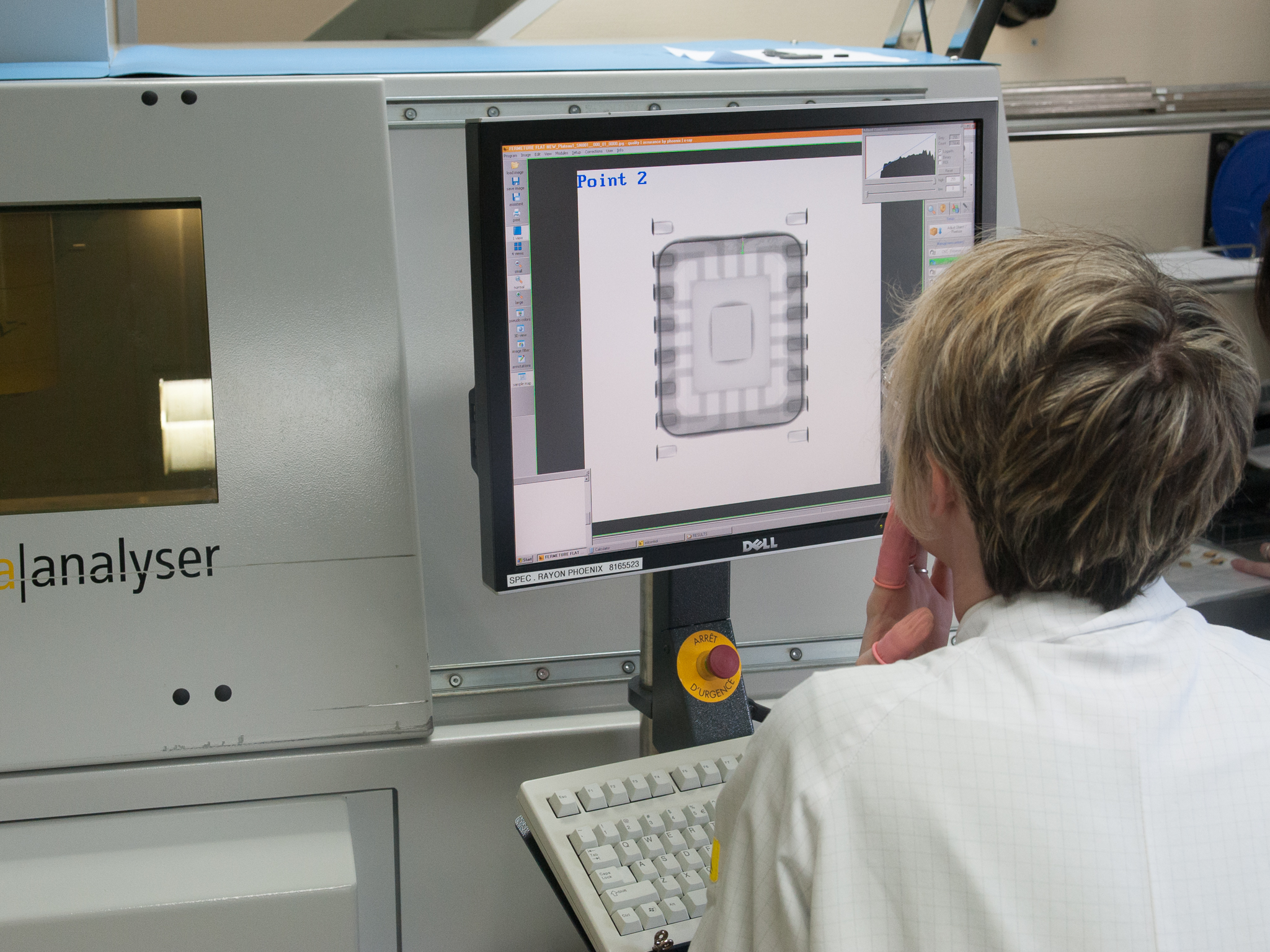
The chips will be X-rayed to check the welds at the interface between the chip and the carrier and the weld joint between the upper and lower half of the package to ensure that there are no voids in the welds.
The testing also checks for the presence of particles inside the packages, since the tiniest grain of dust would have disastrous consequences. Each package is also tested with a leak detector.
Get Tom's Hardware's best news and in-depth reviews, straight to your inbox.
The chips are also subjected to a certain number of thermal cycles (between -55 degrees Celsius and 125 degrees Celsius, or -67 degrees Fahrenheit to 257 degrees Fahrenheit) and thermal shocks. At each stage, STMicroelectronics checks the electrical performance of the dies and a test report is kept for each chip produced. At the end of the process, the result is a component that Patrick Galloy calls a “one-of-a-kind little jewel.” Each die is marked with a unique serial number that makes it possible to track its life since the start of fabrication, part by part, chip by chip, and test by test. All results are sent to the customer, and also archived for at least 10 years.
STMicroelectronics preferred not to disclose the number of functional chips that leave the Rennes fabrication facility (that data is currently kept secret). But it’s easy to see that the yields have to be significantly lower than in a more traditional fab that isn’t subject to the same constraints and destructive tests for guaranteeing the quality and reliability of the chips.
Current page: Highly Rigorous Tests
Prev Page A Demanding Selection Process Next Page Operations At The Site-
Scionyde "The poor overall economic picture and pessimistic approach newspapers like to take in speaking of the electronics industry in France would lead you to think that that scenario is utopian at best."Reply
Maybe I'm missing something obvious, but isn't 'utopian' the exact opposite of the word you were intending to use there? -
vancedecker This is really cool. A totally unexpected article in the swamp of cell phone reviews and press releases, on other sites...Reply -
army_ant7 @ScionydeReply
I'm thinking that "utopian" was used in a way to mean something highly unachievable, unlikely, or unfeasible. I'm not sure how that would apply though and I can't speak for the author. I'm not sure if this helps explain that... -
vaughn2k "Once the die is mounted in its case, the wires must be soldered to connect the chip and the pins. This operation can seem archaic compared with the processors used in PCs or smartphones, whose dies are connected via direct contact with bumps on their epoxy carriers." - The wire is not soldered to the pins but welded using an ultrasonic force + power - or Ultrasonic wirebonding. The head of the tool where the wire (either it is an Al or Au wire) comes out, generates this combination of ulrasonic energy to be able to connect the die pad and pins. If an Au wire is used, the process adds a thermal property, which is also called thermosonic bonding. CPU and smart phone chips (and virtually all chips) uses the same process. However, most assembly uses Au wire or Cu wire, instead of Al wire. Another process that is used o intorconnect chips to substrate is called flip-chip bonding, or soldering or ILB (inner lead bonding), and then going into the process of underfilling, to protect these interconnects.Reply -
vaughn2k "The testing also checks for the presence of particles inside the packages" - It is called PIND test (Particle Impact Noise Detection). It is in MIL-STD 883E method 2020.8 -- ;)Reply -
WyomingKnott What double-post? I don't see one.Reply
More practically, you should be able to delete your own post by going to the forum version of the comments. Click on the blue icon with quotation marks, full-edit the duplicate post, and there should be a delete button. -
Hey, and what about Goodram? Isn't it the last european based manufacturer of ram, flash, ssd etc? Can you please make a small trip there as well?Reply


