Inside Intel's Secret Overclocking Lab: The Tools and Team Pushing CPUs to New Limits
We get an exclusive tour of the facility where Intel pushes chips to their absolute limit.

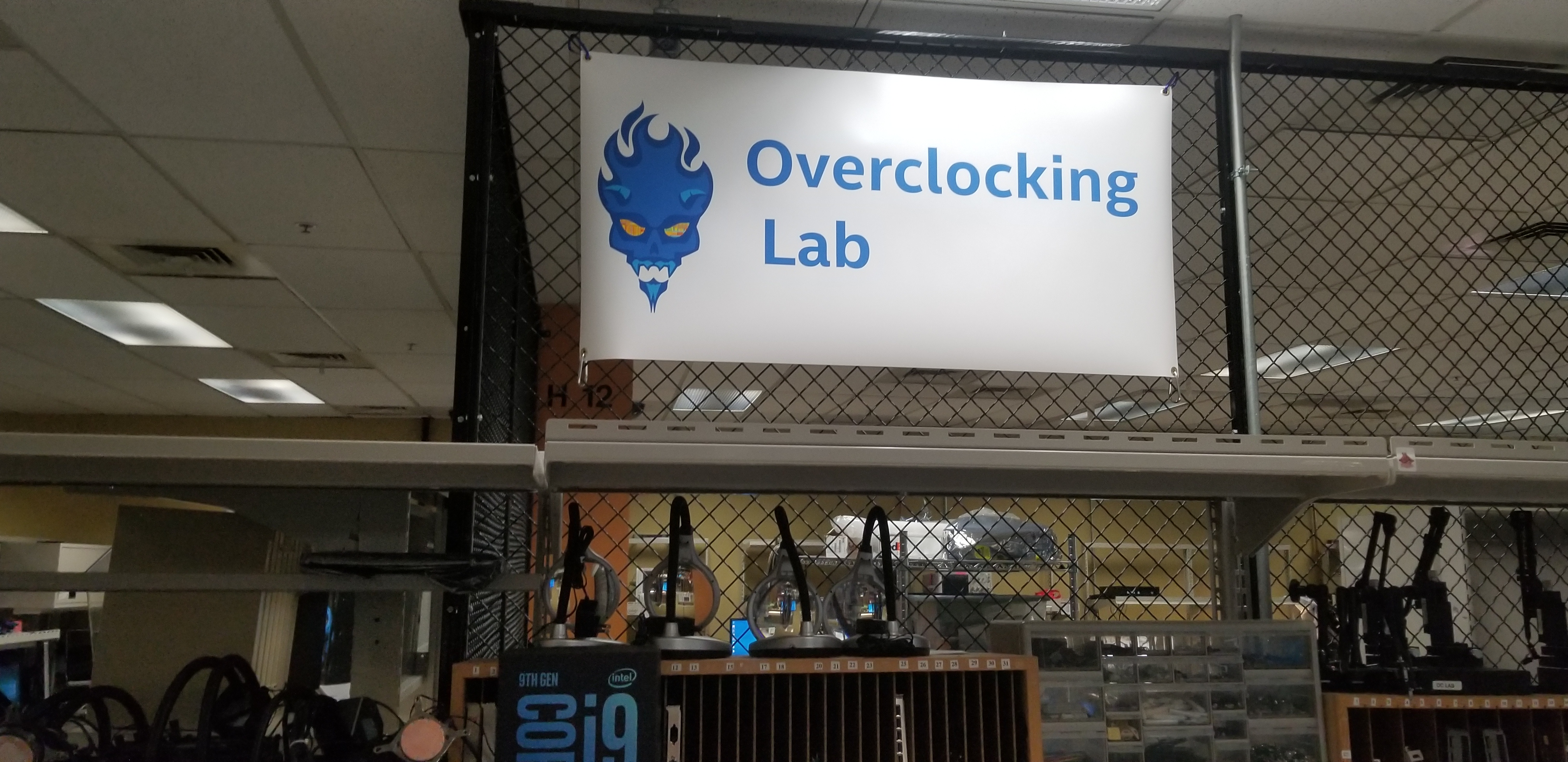
Intel says it loves overclocking, but saying it and proving it are two different things entirely. We here at Tom's Hardware certainly love overclocking, so we visited Intel's Jones Farm campus in Portland, Oregon, recently for an exclusive tour to see how the company designs and architects its chips for maximum overclockability.
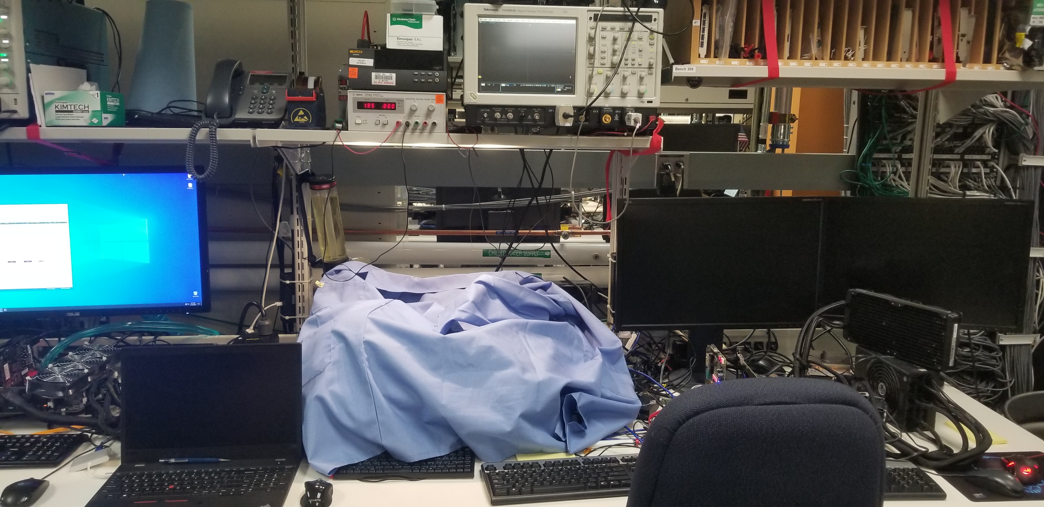
Intel's overclocking lab has silently steered the company's overclocking efforts for years and, understandably, the company has been hesitant to open it up to the media. To our knowledge, we are the first tech news outlet to visit and report on the facility. As we can see below, the lab is packed with next-gen gear that the company isn't ready to divulge, some of it hidden under Intel-blue lab coats for our visit.
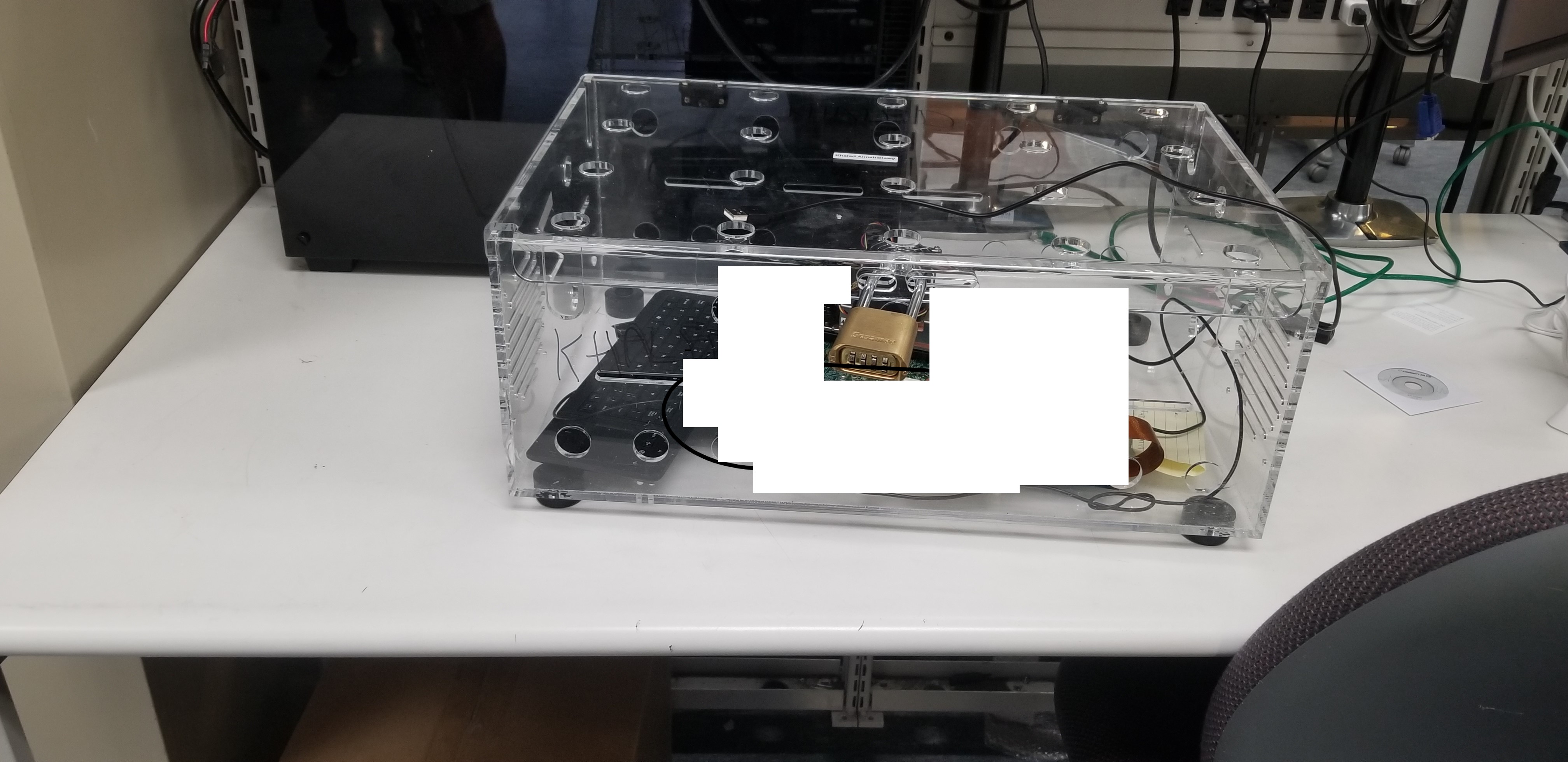
Security is an everyday concern at Intel, and as part of its standard operating procedures, sensitive gear is kept in locked Plexiglas cases in most of the building when it isn't actively being tested. The cases are large enough to make it difficult, if not impossible, to ferret hardware out of the building unnoticed. Inside of the confines of the OC lab, which is protected by a keypad entry system, the technicians can operate with a bit more freedom.


Intel is certainly a company at a crossroads: After more than a decade of dominance, it is pressured by AMD with its Ryzen processors that offer leading performance in key metrics, and at ultra-competitive pricing that challenges Intel's desktop PC dominance.
Much of AMD's advantage lays in TSMC's 7nm process, which is denser and more efficient than Intel's go-to 14nm node. But overclocking headroom remains an advantage for Intel, as its chips have much more margin between the rated boost frequencies and overclocked clock rates than AMD's processors.
Make no mistake, AMD has done a great job of extracting the utmost performance from the new 7nm node, but the fact remains: The industry is grappling with stagnant, if not declining, clock rates from process nodes as they shrink further, leading many to question if overclocking is dead.
During our visit, we discussed the labs' role and procedures, examined the gear, asked Intel's team about the future of overclocking, and peppered them with questions about some of the important concerns on the minds of overclockers, like safe voltage guidelines and the impact of overclocking on chip longevity.
Get Tom's Hardware's best news and in-depth reviews, straight to your inbox.
Move the Bits Faster
Overclocking is all about pushing the bits inside the processor faster by altering it to operate beyond the rated specifications. It sounds simple enough, but as enthusiasts know, what appears to be a rather straightforward exercise can be extremely complex, especially if you're pushing the extreme edge of performance.
As challenging as wringing the utmost performance out of silicon can be, it's nothing compared to the complexity of designing and integrating that functionality into products that begin their life as grains of sand. Consider this: At 5 GHz, the nanometer-scale transistors inside today's modern chips switch on and off at a rate of five billion times per second, and that isn't even the pinnacle of performance – it isn't uncommon to see speeds over 7 GHz with liquid nitrogen cooling.
Exposing that hidden performance to enthusiasts and casual users alike presents tremendous challenges for the engineering teams tasked with ensuring the billions of transistors on your chip can survive the rigors of elevated voltages and temperatures that come as a byproduct of overclocking.
That's one of the fundamental reasons why Intel created its Overclocking Lab, a team of engineers led by Dan Ragland, the Principal Engineer of Performance Tuning & Overclocking Architecture. The team is tasked with not only exposing new overclocking features to users but also tracking silicon quality, voltage scaling and conducting long-term stress testing, all of which help the company improve its processors for all users – even those that aren't interested in overclocking.
The overclocking lab operates in relative secrecy as far as the public is concerned, but it is just down the hallway (and to the right) from where we attend Intel's annual data center briefings, so it isn't necessarily hidden inside Intel's Jones Farm campus in Portland, Oregon.
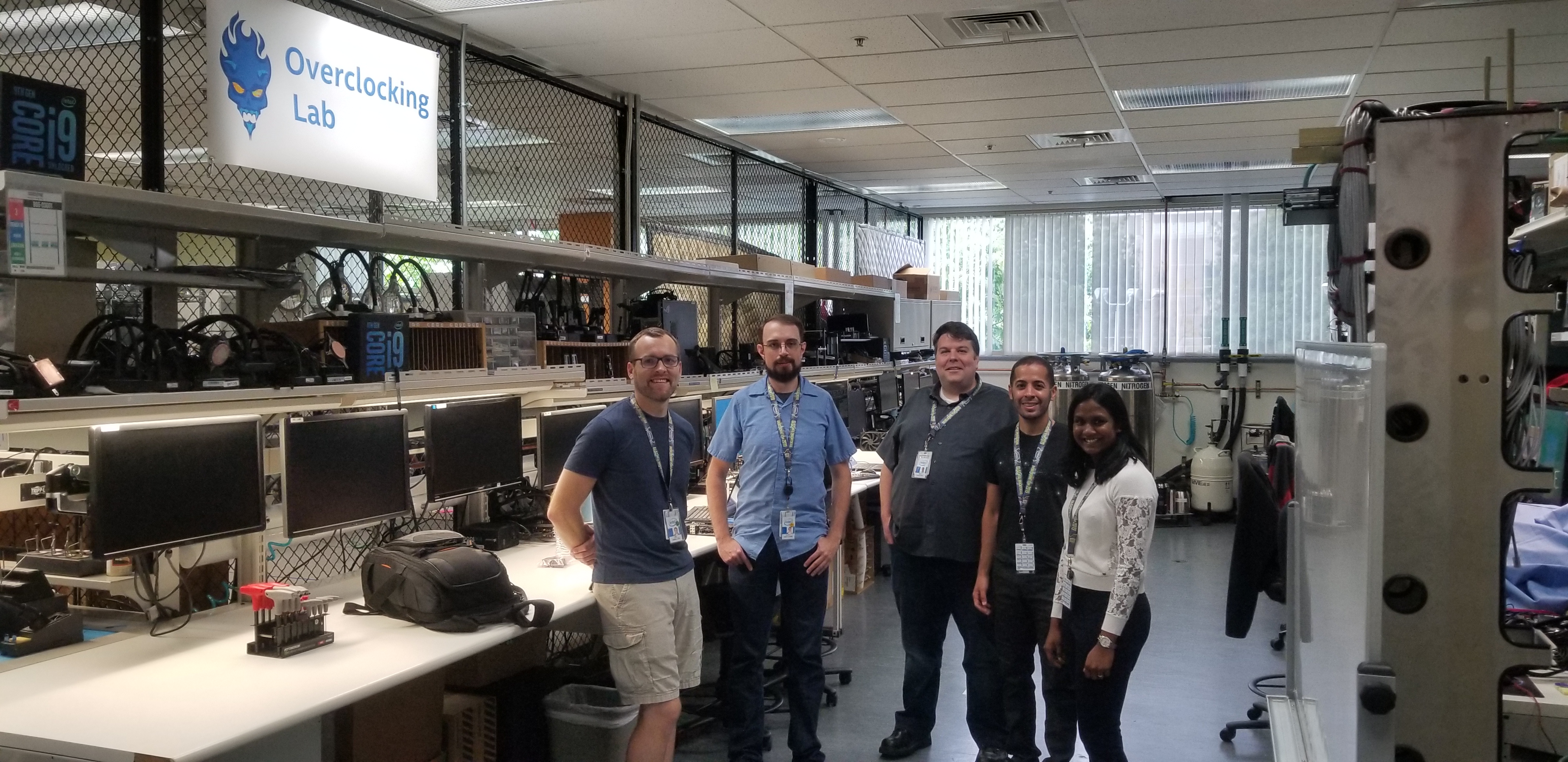
For our tour, Ragland was joined by four members of his eight-person engineering team that he handpicked for their experience in multiple disciplines, from mechanical/thermal engineering to software. Ragland selects from among the best the company has to offer, but aptitude and enthusiasm are key traits he looks for when selecting team members. A passion for overclocking is a ground-floor requirement to make the team.
A group of eight engineers seems like a small number of engineers dedicated to overclocking performance for a company with a market cap of ~$250 billion, but this team interacts with multiple other groups, from Intel's Israel-based IDC team during the design phases of processor architectures to the teams responsible for power code management and overclocking software, among many others.
The team also interfaces with motherboard vendors to help them optimize their platforms for overclocking, part of which includes overclocking workshops that we'll cover shortly. Intel also regularly brings in leading overclockers from around the world to work with them in the lab to help the company better understand the challenges of overclocking, and address issues.
We asked during our tour if the lab also does competitive performance analysis of competing products, like testing AMD's chips for comparison, "We're very aware of our competition, but we can't say much beyond that," Ragland responded.
We'll dive in on the history and rationale behind Intel's overclocking initiatives on the following page, then dive in deeper on the tech behind the scenes.
- PAGE 1: The Overclocking Lab
- PAGE 2: The Beginnings and Mission of Intel's Overclocking Lab
- PAGE 3: Pouring LN2, the OSHA Way
- PAGE 4: TIM, Coolers, The Medusa, and Other Intel Lab Gear
- PAGE 5: Validation Boards and Overclocking Bootcamps
- PAGE 6: VRM Supercooling, PCH Swapping, and Internal Tools
- PAGE 7: 'Safe' Overclocking Voltages and Techniques
- PAGE 8: Is Overclocking Dead?
MORE: Best CPUs
MORE: Intel & AMD Processor Hierarchy
MORE: All CPUs Content
Current page: The Overclocking Lab
Next Page The Beginnings and Mission of Intel's Overclocking Lab
Paul Alcorn is the Editor-in-Chief for Tom's Hardware US. He also writes news and reviews on CPUs, storage, and enterprise hardware.
-
Paul Alcorn ReplyDark Lord of Tech said:Can you get the AMD tour? Would love to see that.
I'll jump on a plane the second it is offered :) -
bit_user @PaulAlcorn , thanks for the awesome piece!Reply
I'm still making my way through it, but wanted to draw special attention to this bit:
the engineers told us they feel perfectly fine running thier Coffee Lake chips at home at 1.4V with conventional cooling, which is higher than the 1.35V we typically recommend as the 'safe' ceiling in our reviews. For Skylake-X, the team says they run their personal machines anywhere from 1.4V to 1.425V if they can keep it cool enough, with the latter portion of the statement being strongly emphasized.
Thanks for that!
At home, the lab engineers consider a load temperature above 80C to be a red alert, meaning that's the no-fly zone, but temps that remain steady in the mid-70’s are considered safe. The team also strongly recommends using adaptive voltage targets for overclocking and leaving C-States enabled. Not to mention using AVX offsets to keep temperatures in check during AVX-heavy workloads. -
StewartHH Some one should comparison between different vendors die size like Intel 10nm vs AMD 7nm to see if there is actually performance gain. I would use per-core speed and not taking multiple cores into account.Reply -
bit_user @PaulAlcorn , uh oh. Now that I just finished heaping praise, I've got a gripe. In the penultimate paragraph:Reply
... assures that the learnings lessons and advances made in the overclocking realm ...
I was saddened to see the "learnings" virus infecting your otherwise admirable writing.
I think "learnings" is one of those pseudo-jargon words that MBAs and other B-school types like to throw around, out of jealousy for practitioners of real professions. Everyone from auto mechanics to accountants, lawyers, and doctors needs jargon to adequately and efficiently express concepts and constructs central to their work. However, common sense pervades business to such a degree that I think they're embarrassed by how easily understandable it'd be, if they didn't inject some fake jargon to obscure the obvious. The resulting assault on the English language is disheartening, at best.
Yes, if you've ever heard of her, you probably guessed I'm a fan of Lucy Kellaway, former journalist of the Financial Times and BBC. Worth a read:
The 8 Lucy Kellaway rules for claptrap and the fundamental theorem of corporate BS
Lucy Kellaway’s dictionary of business jargon and corporate nonsense -
Gurg AMD CTO Mark Papermaster: "you can't rely on that frequency bump from every new semiconductor node." AMD's future outlook of very limited frequency bumps, performance increases only from more cores and expensive software modifications to use more cores.Reply
VersusIntel Ragland: "People who think this the end of the world for overclocking because our competitors' 7nm has very little headroom, that's not true. Intel is all about rock-solid reliability; our parts aren't going to fail...you can count on your part running at spec, so there's so much inherent margin that we will always have overclocking headroom...I think users will be happy with the margin we can offer in the future."
Ouch! Intel's Ragland really "punked" AMD's negative outlook.
PS Great fascinating article -
jiang-v Anyone knows how to made contact with them? cause I fould a big bug on 10th corex chip about adaptive mode overclockingReply
overclocking/comments/ehxa7cView: https://www.reddit.com/r/overclocking/comments/ehxa7c/big_bug_in_10th_core_x_vid_mechanism_worst_avx512/ -
nofanneeded In the past OC gave a huge difference , today we can easy hit 4.4 all cores without OC and this is more than enough for me.Reply
for me OCing is dead. and I dont care about missing 5 fps.
I put the price difference in a better GPU ... -
CompuTronix Outstanding article! Thank you, Paul! I would love to have been there. I have a few dozen questions that the Team may or may not have been allowed answered.Reply
However, like bit_user, I found it of particular interest that the Team was forthcoming regarding specific voltage and temperature values they're comfortable with running on their personal home rigs, which max out at 1.425 and 80°C. With respect to electomigation and longevity, every day in the forums we see many overclockers express their concerns over these very issues.
On their website, Silicon Lottery shows Historical Binning Statistics that include the Core voltages used to validate their overclocked 14 and 22nm processors. For 22nm the maximum is 1.360. For 14nm the maximum is 1.456. While Intel's warranty is 3 years, Silicon Lottery's warranty is 1 year, which suggests at least one reason for the voltage difference between Intel's Team and Silicon Lottery.
Here's a forgotten link to a revealing Tom's Hardware video interview of July, 2016, with Intel's Principal Engineer (Client Computing Group), Paul Zagacki, where BGTnJkuqlbo']Intel Discusses i7-4790K Core Temperatures and Overclocking. The video coincides with the formation of Intel's Overclocking Lab, also in 2016. In the video, Intel points out that overclocking abilities begin to "roll off" above 80°C, which agrees with the value the Team revealed in your article.
While Core temperatures, overclocking and Vcore are often highly controversial and hotly debated topics in at least the overclocking forums, the term "electromigration" is closely related to a much less known term, which is "Vt (Voltage threshold) Shift". With respect to voltage and temperature, the two terms describe the causes and effects of processor and transistor "degradation" at the atomic level.
In the Intel Temperature Guide, in Section 8 - Overclocking and Voltage, I created a table for Maximum Recommended Vcore per microarchitecture from 2006 to the present. For 22 and 14nm, those values are 1.300 and 1.400 respectively. I also created a graph showing the Degradation Curves for 22 and 14nm processors. The table and graph helps overclockers get a better perspective of the degradation and longevity issue:
Sparing our members and visiting readers the deep dive, Vt Shift basically represents the potential for permanent loss of normal transistor performance. Excessively high Core voltage drives excessively high current, power consumption and Core temperatures, all of which contribute to gradual Vt Shift over time. Core voltages that impose high Vt Shift values are not recommended. The 14nm curve suggest 1.425'ish is the practical limit, which also agrees with the value the Team revealed in your article. The curve also suggests that Silicon Lottery might be pushing the edge of the envelope a bit.
The concern here is that when novice overclockers casually glance around the computer tech forums, where conflicting and misleading numbers get flung around like gorilla poo in a cage, many don't realize through the fog of all the confusion that one size Vcore does not fit all. Aside from high Core temperatures, Vcore that might be reasonable for one microarchitecture can degrade another. So 22nm Haswell users now wanting to overclock their aging processors to keep up with today's games need to heed the degradation curves, which applies as well to 14nm Skylake and Kaby Lake users.
CT :sol:
