Introduction


It's less than three years ago when I received an email from the at this point rather unknown company called 'nVIDIA' in July 1997, asking me if I was an 'enthusiastic hardware reviewer' who would like to have an in depth look at their new 3D video chip called 'RIVA128. At this time I hadn't done any 3D card reviews at all and my knowledge of 3D was rather mediocre. I answered with a big YES and received my first 3D card sample in August 1997, starting off a 3D review section at Tom's Hardware Guide as well. Since this time we both have come a long way. Tom's Hardware Guide is still the largest hardware review site on the Internet, leading with double the amount of readers and page requests of its next competitor and NVIDIA has made it to the top of 3D chip makers, after pushing 3dfx from its throne more than a year ago. Since NVIDIA's IPO the stock price (Nasdaq: NVDA ) has been continuously raising to reach an incredible level since it was announced that NVIDIA will provide the 3D chip for Microsoft's X-Box.
NVIDIA's last 3D chip by the name of 'GeForce256' was the top performer in 3D graphics since its release in October 1999 and until now there hasn't been any product that could threaten GeForce in any way. It was GeForce's huge success that kept NVIDIA from panicking to rush out their next chip, which was available as working silicon already in November of last year. Now the competition is getting ready to release their products to finally give GeForce a run for its money, marking the perfect time for NVIDIA to launch their GeForce2 GTS and raise the bar even further.
However, before we just stand in awe of the impressive numbers that GeForce2 GTS is able to report, we should have a close look at it to find out if the product can live up to the high expectations we have of an NVIDIA product.
What's New?
.18 µm Process Technology
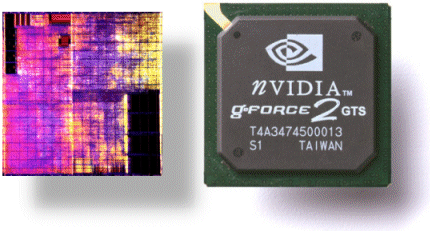
GeForce2 GTS is produced in .18 micron technology, marking a 'shrink' from GeForce's 0.22 micron core. In the world of silicon 'shrinking' is always a huge blessing. It leads to faster switching transistors, thus increasing clock speed, it leads to smaller die sizes, thus reducing production costs, it leads to lower power dissipation, thus reducing the heat produced by the chip and lowering its power consumption. In case of GeForce2 GTS the amount of transistors has been increased by some 2 million to 25 million transistors. Those transistors aren't just there to waste space; they supply the additional features of GeForce2. The power consumption of GeForce2 GTS has halved from the bad 18 W eaten up by GeForce, which led to disaster on so many motherboards with weak power supplies. The power dissipation (which is the amount of power that the chip wastes to heat up our atmosphere) was reduced as well, but GeForce2 GTS still comes with a heat sink and fan of the same size as GeForce, which should give you some kind of idea about GeForece 2's heat production.
The new .18 micron die of GeForce2 is running at a 200 MHz clock, which can be seen as a significant improvement over the 120 MHz of GeForce. As a matter of fact it symbolizes the key factor for GeForce2's superior performance. Unfortunately advances in DDR-SDRAM technology haven't been as great. GeForce2 is using DDR-memory running at 166 MHz (practically 333 MHz) vs. the 150 MHz (practically 300 MHz) memory clock of its predecessor GeForce, since there's no faster memory available right now. This means a 66% increase in core clock, but a mere 10% increase in memory clock, translating in an at least 66% faster T&L and rendering engine that has to cope with an only 10% higher memory bandwidth of 5.3 GB/s. If GeForce used to have memory bandwidth problems already, GeForce2 GTS will have worse.
'2nd Generation GPU' ..?
Mainly this is an improved version of the TnL-engine of GeForce, obviously clocked at 200 MHz, thus 66% faster than GeForce's 15 million triangles/s and logically leading to a TnL-performance of 25 million triangles/s. I am failing to see what makes this 'GPU' ('geometry processing unit') 'second generation'.
After all even Intel doesn't call a processor running at higher clock speed '2nd generation' as well. Still we've got to give NVIDIA one thing. They were the first to come out with an integrated TnL-engine and GeForce2GTS is no less than the second chip with a working integrated TnL-engine, no matter if you call it 1st, 2nd or 'nth' generation.
S3's Savage2000 chip that was released at the end of the last millennium may be noted in history as the first and hopefully only 3D chip with a purely cosmetic, but never working integrated TnL-engine, which we might call the 0th, -1st or maybe simply 'lost' generation 'GPU'.
ATi is trying its luck on putting an integrated TnL-engine into their upcoming 'Radeon256' chip, which supposedly will be able to deliver 30 million triangles/s. ATi is world famous for claiming numbers that are sky high, alas often failing to deliver actual performance in the end. We will see how this 'Charisma Engine' will feed 30 million triangles/s into two rendering pipelines that can only produce 400 Mpixels/s. Until then, NVIDIA is the first and the last supplier of mainstream 3D chips with integrated TnL.