Steam Deck's custom AMD processor exposed — Van Gogh die shots reveal CPU, GPU core designs, and unused hardware
Van Gogh is a very unique AMD chip.

Get Tom's Hardware's best news and in-depth reviews, straight to your inbox.
You are now subscribed
Your newsletter sign-up was successful
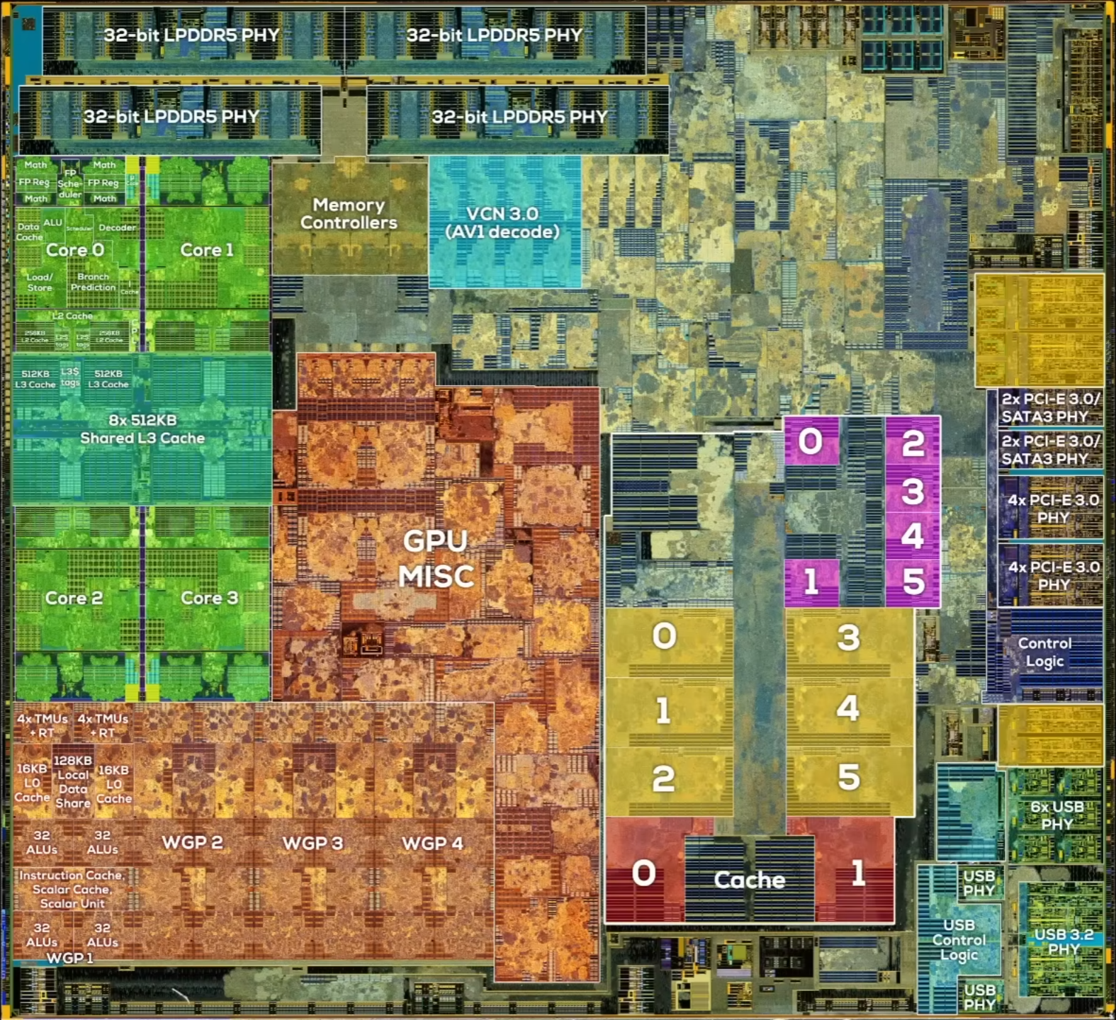
YouTuber High Yield and photographer Fritzchens Fritz have released an in-depth analysis of the 7nm Van Gogh APU found inside the original Steam Deck, featuring die shots with annotated components. The study revealed the layout of the Van Gogh APU and how significant each component is and cleared the air on some hardware that seemingly served no purpose for the Steam Deck.
Codenamed Aerith by Valve, Van Gogh is an APU designed by AMD and manufactured on TSMC's 7nm process. It contains four Zen 2 cores and eight RDNA 2 Compute Units (CUs), which is relatively underpowered compared to mainstream Ryzen APUs for laptops. Van Gogh isn't available for any company as a semi-custom design, hence its near-exclusive use in the Steam Deck.
The die-shot analysis confirmed these basic specs and revealed how significant each component inside the APU was. Van Gogh measures 162mm², with the LPDDR5 memory buses using about 9%, CPU cores taking up 12%, and the GPU cores consuming 11%. Of note, the GPU cores themselves only make up roughly half of the entire graphics processor. Miscellaneous GPU functions and components combined are approximately the same size as the eight RDNA 2 CUs.
Article continues belowCombined with the memory controller and other GPU-related components, these parts comprise only half of Van Gogh's total size. I/O components for USB ports and display capability are contained within the other half, but the die shots show many unaccounted areas remaining.
According to High Yield, 13% of the Van Gogh APU's space is dedicated to a component he initially couldn't identify but believes is the computer vision processing engine (CVPE) used inside the Magic Leap 2 AR headset. The Magic Leap 2 is confirmed to use AMD's Mero APU, which has four Zen 2 cores and eight RDNA 2 CUs like Van Gogh. Initially assumed to be a variant of Van Gogh, High Yield claims Van Gogh and Mero are the same chip used in both the Steam Deck and Magic Leap 2.
One vital piece of evidence for this claim is that the 6nm Sephiroth APU used in the Steam Deck OLED is much smaller than the 7nm Aerith chip. Although TSMC's 6nm has 18% denser logic transistors than 7nm, Sephiroth's 20% smaller size implies that something was removed to slim down the new APU.
High Yield further speculates that original Steam Decks may be able to utilize the CVPE hardware that currently goes unused. However, that depends on whether AMD manually disables the CVPE using a laser or if it's merely turned off by firmware. It's also not clear how well modders would be able to utilize the CVPE since it's used exclusively in Magic Leap hardware and software.
Get Tom's Hardware's best news and in-depth reviews, straight to your inbox.

Matthew Connatser is a freelancing writer for Tom's Hardware US. He writes articles about CPUs, GPUs, SSDs, and computers in general.
-
bit_user ReplyHowever, it uniquely has four memory channels instead of the usual two, which enables greater bandwidth.
I wondered... but this turns out to be a "nothing burger". It's just referring to the way DDR5 has 32-bit subchannels. Just like mainstream desktop CPUs, this thing has a 128-bit datapath.
https://chipsandcheese.com/2023/03/05/van-gogh-amds-steam-deck-apu/
So, no. Nothing "uniquely" about it. You can even see that much from the annotated diagram in this article: 4x "32-bit LPDDR5 PHY" = 128-bits.
claims Van Gogh and Mero are the same chip used in both the Steam Deck and Magic Leap 2.
Holy cow! I didn't even realize Magic Leap was still a going concern! Yeah, this does seem quite anemic for a high-end AR device. It's nowhere close to what Apple's got in the Vision Pro.
It's also not clear how well modders would be able to utilize the CVPE since it's used exclusively in Magic Leap hardware and software.
Would be interesting if it turns out to be some off-the-shelf Xilinx IP. It's probably off-the-shelf from somewhere (MS used Tensilica DSP cores, in Hololens' SoC). It wouldn't make sense to design a full-custom block just for that, due to all the software toolchain and additional validation that would be needed. -
usertests Reply
Luckily it doesn't have 64-bit, like the similar Mendocino appears to have.bit_user said:I wondered... but this turns out to be a "nothing burger". It's just referring to the way DDR5 has 32-bit subchannels. Just like mainstream desktop CPUs, this thing has a 128-bit datapath. -
-Fran- The other way to read this is that Valve has had plenty of time to play around with this SoC and see how they can use it in their next HMD. Or that is the dream?Reply
Regardless, it ties in well with the SteamVR 2.0 rehaul making it, basically, the same SteamDeck UI.
Interesting findings and some hopium into Valve putting out a proper Enthusiast VR HMD and not a Apple-fied expensive piece of junk.
Regards.
