
Intel is clearly behind its rivals TSMC and Samsung with the first generation of extreme ultraviolet (EUV) lithography technology, but it certainly wants to be the first to adopt the next-generation EUV tools featuring a 0.55 NA (or high-NA) that provides higher resolution and productivity. This week Intel announced that it had ordered its second experimental High-NA tool from ASML.
Intel announced plans to adopt ASML's High-NA Twinscan EXE scanners for high-volume manufacturing (HVM) starting in 2025, which is when the company intends to start using its 18A (~1.8 nm) fabrication technology. To do so, Intel has experimented with High-NA tools since 2018 when it obtained ASML's Twinscan EXE:5000, the industry's first EUV scanner with a 0.55 numerical aperture. This week the company ordered ASML's next-generation High-NA tool, the Twinscan EXE:5200.
"Compared to the current EUV systems, our innovative extended EUV roadmap delivers continued lithographic improvements at reduced complexity, cost, cycle time and energy that the chip industry needs to drive affordable scaling well into the next decade,” said ASML President and CTO Martin van den Brink.
Article continues below
High-NA EUV tools are crucial for higher resolution (<8 nm vs ~13 nm for 0.33 NA EUV) that enables smaller transistors and higher transistor density. In addition to a completely different optics design, High-NA scanners promise to offer significantly faster reticle and wafer stages as well as higher productivity. For example, the productivity of the ASML Twinscan EXE:5200 is over 200 wafers per hour (WPH). In contrast, ASML's top-of-the-range 0.33 NA EUV machine, the Twinscan NXE:3600D, produces around 160 WPH with a 13.5nm light wavelength.
"Intel's focus is to stay at the forefront of semiconductor lithography technology and we’ve been building our EUV expertise and capacity over the last year," said Dr. Ann Kelleher, executive vice president and general manager of Technology Development at Intel. "Working closely with ASML, we will harness High-NA EUV's high-resolution patterning as one of the ways we continue Moore's Law and maintain our strong history of progression down to the smallest of geometries."
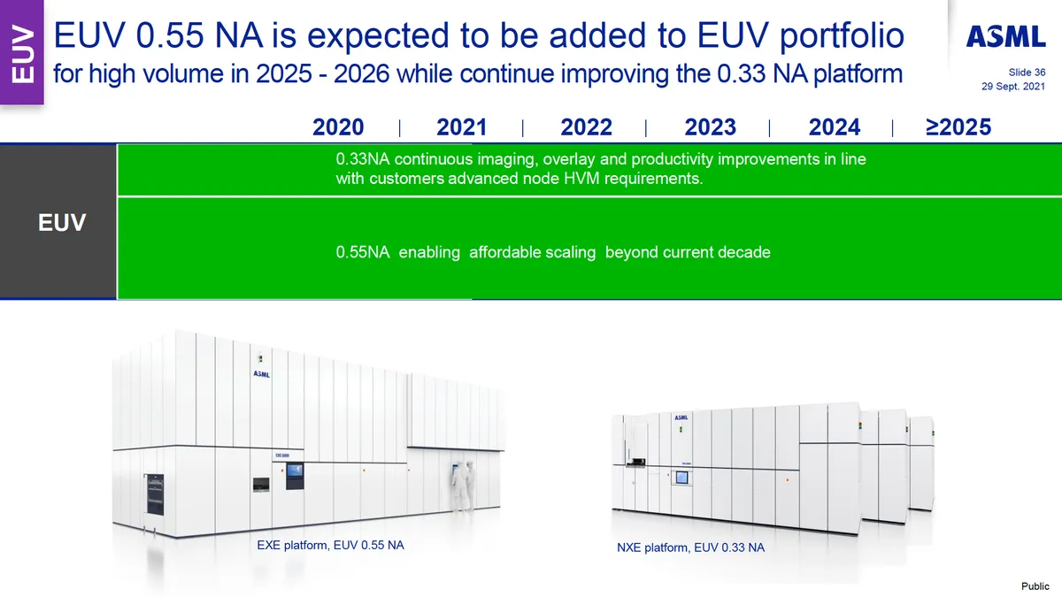
Just like the adoption of 0.33 NA EUV did not eliminate the usage of deep ultraviolet (DUV) lithography, 0.55 NA EUV will not replace the existing DUV and EUV tools used in modern fabs. In fact, ASML plans to continue developing more advanced DUV and 0.33 NA EUV scanners for years to come. Meanwhile, High-NA EUV lithography will be a key technology to reduce transistor sizes and increase transistor density.
