
Introducing GM204: There's A New Maxwell In Town
Nvidia introduced its newest graphics architecture, code-named Maxwell, about seven months ago in the mid-range GeForce GTX 750 and 750 Ti. While those cards don't deliver the high performance of a flagship gaming rig, they introduce unheard of energy efficiency to the PC graphics space. The Maxwell-powered GeForce GTX 750 Ti is a poster child for great performance per watt, achieving frame rates on par with graphics cards doubling its 65 W thermal ceiling.
The company gets there by applying the same advancements made to its Tegra family on GeForce, maximizing what each piece of a GPU can do given an unforgiving power budget. But enthusiasts don’t really lust over efficiency alone. Mostly, they want breakneck speed. And we’ve wanted a performance-oriented implementation of Maxwell ever since the GeForce GTX 750 Ti surfaced. Guess what Nvidia’s giving us today? Its GeForce GTX 980 and 970. If you game, this is the Maxwell you've been waiting for.

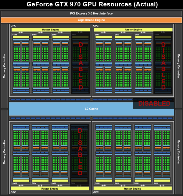
From a high level, the GM204 GPU in these cards looks like the GeForce GTX 750 Ti's GM107, scaled up appropriately. Like GM107, it leverages four partitioned blocks per Streaming Multiprocessor (SMM). Each SMM plays host to 128 CUDA cores, 32 load/store units, eight texture units, and a single PolyMorph engine. Two megabytes of L2 cache is shared across the entire GPU. The obvious difference, though, is the number of SMMs: while GM107 has five, the GeForce GTX 980’s GM204 features a staggering 16 of them. That adds up to a total of 2048 CUDA cores, 512 load/store units, 128 texture units, and 16 PolyMorph engines. Naturally, the second-fastest GeForce GTX 970 has some of those resources disabled, totaling 13 SMMs, 1664 CUDA cores, 416 load/store units, 104 texture units, and 13 PolyMorph engines.

Despite their similarities, the GM204 benefits from a lot of upgrades compared to GM107. For example, each SMM in the GeForce GTX 980 has a 96 KB chunk of shared address space for compute tasks, up from the 750 Ti's 64 KB. The new GPU's L1/texture cache size is now 24 KB per pair of CUDA core processing blocks (48 KB per SMM), doubling GM107.
Unlike GM107, the GM204 GPU features four Graphics Processor Clusters (GPCs) instead of one. That means it benefits from four times the number of raster engines. Of course, high-end graphics cards require a beefier back-end to handle all of that data throughput, and the GeForce GTX 980 utilizes four render back-ends capable of handling 16 full-color ROP operations per clock, adding up to 64. Four 64-bit memory controllers create an aggregate 256-bit bus. By the way, you may have noticed that the GeForce GTX 970's 13 SMMs don't divide equally into four GPCs. Nvidia says that there is no predefined recipe of SMMs per GPC in the 970, and each GPU may be configured differently.
The GeForce GTX 980 runs at a 1126 MHz base clock rate with a rated 1216 MHz GPU Boost frequency, while the GeForce GTX 970 has a 1050 MHz base and 1178 MHz typical GPU Boost rate. Both models carry 4 GB of GDDR5 RAM set to 1750 MHz, or 7 GT/s, yielding 224 GB/s of theoretical bandwidth.
[ADDENDUM]: Since we published this review, it's come to light that the GeForce GTX 970 has more limitations than Nvidia originally disclosed. While the GTX 980 sports 2MB of L2 cache, the 970 is limited to 1.75MB. The GTX 980 features 64 ROPs, but the 970 is limited to 56 thanks to a partially-disabled cluster. In addition, the 970's memory is segmented into 3.5GB and 500MB chunks with 196 GB/s and 28 GB/s of bandwidth, respectively. Since these chunks can not be striped, the maximum usable memory bandwidth for the 3.5GB chunk is is 196 GB/s, not 224 GB/s as originally reported. For more information, see our update article The Real Nvidia GeForce GTX 970 Specifications. [/addendum]


It probably makes the most sense to compare GM204 to the Kepler-based GK110 in Nvidia’s GeForce GTX 780 Ti, even if we know it probably won’t go down in history as the most potent GPU based on Maxwell. The 780 Ti has 2880 CUDA cores, 240 texture units, 48 ROPs, and a 384-bit aggregate memory bus with 336 GB/s of memory bandwidth. Every one of those attributes (except for ROPs/clock) overpowers the GeForce GTX 980's specifications. But keep in mind that Maxwell is a more efficient architecture able to do more with fewer resources. For a quick refresher, you may want to have a look at our GeForce GTX 750 Ti Review: Maxwell Adds Performance Using Less Power.
The point is that we expect GeForce GTX 980 to compete on the 780 Ti's level, maybe even beating it. The GeForce GTX 980’s raster processing appears particularly well-endowed, with 64 full-color ROPs per clock and 72 Gpixels/second of fill rate. Compare this to the GeForce GTX 780 Ti's 48 ROPs per clock and 44 Gpixels/s. That should give GM204 an edge when it comes to high resolutions (like 4K) and anti-aliasing.
Before we go on, though, let's touch on Maxwell's focus on efficiency. Have a look at the GeForce GTX 980's thermal design power limit of 165 W. That's not a typo, and it's almost 100 Watts shy of the GeForce GTX 780 Ti. It's been a long time since we've seen a sub-200 W performance leader in the graphics card world. The GM204's 398 mm2 die size is less than 80% the size of GK110, despite being built on the same 28 nm fabrication node. Consider that this second generation Maxwell GPU is home to 5.2 billion transistors vs Kepler's 7.1 billion. The GeForce GTX 970 is even more of a power miser with a 145 W TDP. If these new GeForce cards can deliver performance on par with their predecessors, Nvidia has accomplished something special.

Regardless of Maxwell’s more efficient graphics architecture, the GeForce GTX 980 suffers a 33% drop in peak memory bandwidth compared to the GeForce GTX 780 Ti. Nvidia mitigates this deficit by implementing an improved memory compression scheme. GM204 sports an improved third-generation delta color compression mode that provides more options to the hardware. Using 8x8 blocks of 64 pixels, compression analysis is performed on 2x4 blocks in order to achieve the best compression possible in 8:1, 4:1, and 2:1 steps. If 2:1 compression isn't doable, that block isn't compressed. Successfully compressed blocks save even more bandwidth every time the memory is read. Nvidia claims that this increases effective memory bandwidth from 224 GB/s to approximately 300 GB/s compared to the GeForce GTX 680 Kepler-class cards. We'll see if this is enough to allow GeForce GTX 980 to stay competitive with the formidable GeForce GTX 780 Ti.
We should mention GM204's upgraded tessellation performance, too. The company's PolyMorph engine 2.0 design was leveraged across Kepler and even the Maxwell-based GM107. But that changes with the GM204's upgraded third-gen PolyMorph engine design. Nvidia representatives claim up to a 50% increase in performance at high tessellation factors per engine due to architectural improvements.

Nvidia's new GPU has some unique display options as well. The GeForce GTX 970 and 980 are the first graphics cards in the world that support the HDMI 2.0 standard, allowing for full 4K support at 60 Hz as an alternative to HDMI 1.2's 30 Hz limitation. The reference card design also includes two DisplayPort 1.2 outputs and a dual-link DVI connector, while the GPU is capable of driving four 4K displays simultaneously using a display engine that supports resolutions up to a forward-looking 5K.
Nvidia also updates its latest GPU with H.265 (HEVC) encoding support, providing a nice future-looking upgrade. As for existing H.264 support, keep in mind that Maxwell's fixed-function video encoder, already available on the GeForce GTX 750, is improved with 2.5x the throughput compared to previous-generation Kepler hardware. Nvidia's ShadowPlay software now features 4K video support at 60 FPS on the GM204, and this capability could possibly be enabled for other Maxwell-based cards in the future.
Nvidia wouldn't tell us whether GeForce GTX 980 is using an uncut version of the GM204 processor, so it's possible that we might see this GPU resurface with even more (or less) CUDA cores in a future product.