3D X-DRAM Roadmap: 1Tb Die Density by 2030
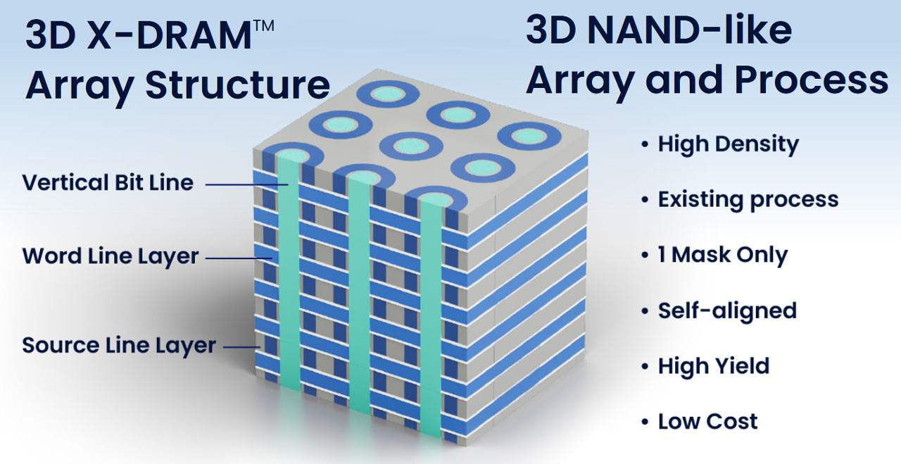
The patented tech will use a 3D NAND-like DRAM cell array structure.

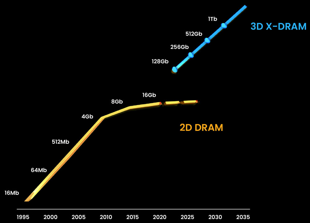
San Jose-based NEO Semiconductor has launched 3D X-DRAM. This patented DRAM technology has the ambitious aim to "solve DRAM’s capacity bottleneck and replace the entire 2D DRAM market." According to company roadmaps, applying 3D NAND-like DRAM cell arrays in DRAM will deliver 1Tb memory ICs by 2030.
1Tb ICs would mean the potential to slap 2TB onto a single DIMM with relative ease — double-sided DIMMs with eight chips per side would get there. 4TB using 32 ICs would also be possible. Obviously that's more for servers than anything consumers are likely to need within the next ten years, with many still getting by with 8GB or 16GB. Note that current memory solutions top out at 128GB per DIMM for registered DDR4 server solutions, using 32 32Gb ICs. Readily available DDR5 registered DIMMs currently offer up to 64GB (32 16Gb ICs), though higher capacity modules are on the horizon.
Again, that's for DRAM, not some kind of Flash NAND. But NEO Semiconductor has developed 3D X-DRAM technology with at least some inspiration from 3D NAND. It uses what is claimed to be "the world’s first 3D NAND-like DRAM cell array" for its capacity boosting USP. There are key differences though, and NEO has already applied for the various patents to protect its IP.


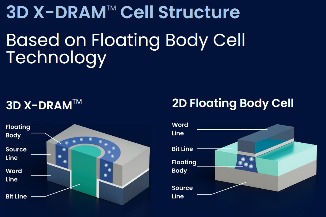
NEO Semiconductor provides a glimpse at how its new 3D X-DRAM works in its press release. The new memory ICs will use a 3D NAND-like DRAM cell array, but we also know that the structure is based upon capacitor-less floating body cell technology. The firm asserts that this change "simplifies the process steps and provides a high-speed, high-density, low-cost, and high-yield solution."
One important aspect contributing to the chances of success are that 3D X-DRAM can be manufactured using contemporary semiconductor fabrication technology. Moreover, the company estimates that "3D X-DRAM technology can achieve 128Gb density with 230 layers, which is eight times today’s DRAM density."
For some perspective on the NEO Semiconductor density claims, Samsung's current highest density DDR5 DRAM ICs are 16Gb in capacity. The South Korean tech firm, an important player in both NAND and DRAM, is expected to launch 32Gb ICs imminently. Combined with chip stacking, that should enable 1TB memory modules in late 2023 / early 2024. That's a lot earlier than NEO's 2030 launch timeframe, and chip stacking for DRAM could go even higher.
Get Tom's Hardware's best news and in-depth reviews, straight to your inbox.

Mark Tyson is a news editor at Tom's Hardware. He enjoys covering the full breadth of PC tech; from business and semiconductor design to products approaching the edge of reason.
-
rluker5 Something like this is going to like good cooling.Reply
I was thinking about going with 64GB DDR5 for no good reason. Now I have even less reason. Money saved for a different upgrade I guess. In a couple years I would be happy to toss some cooling on something like this. -
jeremyj_83 This level of DRAM density would be amazing for virtual hosts. Allowing more local RAM before having to go across the CXL link to a massive pool of high density RAM.Reply -
Kamen Rider Blade I wonder how they will license this patent to the big RAM companies.Reply
Will it be a on a individual company basis, or license through a joint Company/JEDEC agreement? -
Steve Nord_ Reply
Why cooling, I saw nothing on dissipation. I am looking for compute in memory...might take more than 1 mask to have that though.rluker5 said:Something like this is going to like good cooling.
I was thinking about going with 64GB DDR5 for no good reason. Now I have even less reason. Money saved for a different upgrade I guess. In a couple years I would be happy to toss some cooling on something like this. -
Steve Nord_ Reply
...or company mainframe Slack, I guess. HFS on a phone?jeremyj_83 said:This level of DRAM density would be amazing for virtual hosts. Allowing more local RAM before having to go across the CXL link to a massive pool of high density RAM. -
setx AfterReply
This patented DRAM technology
it gets completely uninteresting.
First of all, creating something in a lab and developing cheap mass production are very different things.
Next, and likely more important, various patents with no major manufacturing contracts mean that if they can't put it into next major RAM standard – it's actually going to harm global development, as other companies would avoid the areas covered by patents. -
rluker5 Reply
More capacitors per mm^2 of cooling surface and some have thermal barriers to heat dissipation due to being underneath others.Steve Nord_ said:Why cooling, I saw nothing on dissipation. I am looking for compute in memory...might take more than 1 mask to have that though.
Luckily lots are getting used to ram cooling again.
I just have a dangling fan pointed at mine on the PC that gets the most volts through it. My oc becomes unstable if it gets to 60c. -
InvalidError Reply
Cheap manufacturing may already be a mostly solved problem if the thing is made mostly the same way as NAND, which it probably is.setx said:First of all, creating something in a lab and developing cheap mass production are very different things.
Failing to license the thing at a reasonable price would suck though, as it would likely mean there won't be cheap versions of this stuff until 20 years from now when the patents on whatever makes this meaningfully different from NAND structure expire.
Most of a DRAM chip's ~300mW operating at standard voltage and frequencies is IO, making the chip 32X bigger won't increase IO power much but it might increase self-refresh by ~500mW. 1W per chip should still be well within passive cooling as long as there is room for natural convection around the DIMMs, where there usually aren't when you slap embellishment air-blockers on them that reduce clearance between DIMMs to zero.rluker5 said:More capacitors per mm^2 of cooling surface and some have thermal barriers to heat dissipation due to being underneath others.
The most logical use for this sort of stuff is HBM: all of the advantages without having to do TSVs, die shaving or DRAM die stacking. -
bit_user @InvalidError , good call for predicting this a couple months ago.Reply
1Tb ICs would mean the potential to slap 2TB onto a single DIMM with relative ease — double-sided DIMMs with eight chips per side would get there. 4TB using 32 ICs would also be possible.
It would take an entire minute to read or write 4 TB of DRAM, even at the MCR spec of DDR5-8800 that Intel claims it'll support, in Granite Rapids. I wonder if they'll also have to increase the on-die ECC allocation, to make it viable. -
bit_user Reply
I was thinking about going with 64GB DDR5 for a good reason. The smallest dual-ranked ECC UDIMMs I can find are 32 GB. So, the lowest dual-ranked memory config I can use is 64 GB. That's a good deal more than I need, but at least I won't have to upgrade it for the life of the machine.rluker5 said:I was thinking about going with 64GB DDR5 for no good reason.
When I built a box with 16 GB in 2013, I never had to upgrade the RAM. I only used that much because it's quad-channel and the price difference between 2 GB and 4 GB DIMMs wasn't too bad, at the time.