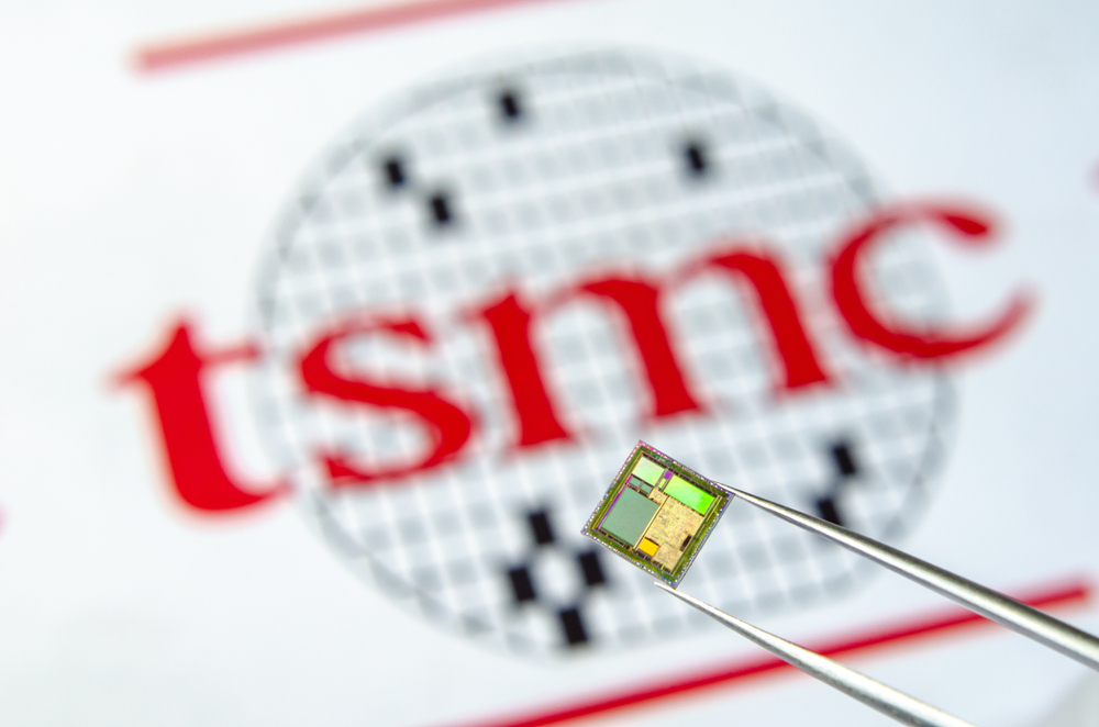
TSMC Starts 2nm Process Development for Fast, Efficient Chips
7, 5, 3, 2, go!
Get Tom's Hardware's best news and in-depth reviews, straight to your inbox.
You are now subscribed
Your newsletter sign-up was successful

At the start of this year we heard that TSMC was investing heavily in 5nm fabrication, and it's no secret that the next step after that is TSMC's 3nm process.The Taiwanese silicon manufacturer is looking beyond that process too, as it just announced to shareholders that it is starting development of its 2nm lithographic process, as spotted by DigiTimes.
Painstakingly few details are available about the 2nm process. All we know is that TSMC is starting development -- though it's safe to assume the end product will be very fast and more efficient than anything on the market today.
Currently, TSMC's 7nm process is in its peak, receiving huge numbers of orders from AMD for its Ryzen 3000-series CPUs and Navi graphics cards. Other customers include Apple, and although Huawei was to be included, that doesn't appear to be working out so well.
On the 5nm front, TSMC is working with EUV lithography, similar to what Samsung is accomplishing. The two chipmakers are neck-in-neck in the silicon race. According to DigiTimes, TSMC is expecting 10% of this year's revenue to come from its 5nm EUV lines.
After that, the 3nm process will take over, and TSMC expects mass production to start in 2022.
Meanwhile, TSMC's CoWoS production lines are also reportedly at full capacity, packaging chips with multiple dies side-by-side onto single silicon interposers using a 2.5D packaging method.
Get Tom's Hardware's best news and in-depth reviews, straight to your inbox.
Niels Broekhuijsen is a Contributing Writer for Tom's Hardware US. He reviews cases, water cooling and pc builds.
-
derekullo According toReply
https://en.wikipedia.org/wiki/Atomic_radius
The atomic radius of silicon is 110 picometers or 0.11 nanometers.
I'm highly curious how they intend on dealing with fabrications approaching 0.11 nanometer.
We have come a long way since the 3 micrometer (3000 nanometer) 8086. -
hannibal we have to remember that ”7nm” is in reality 54nm so we Are not even near Atom level sizes. Marketing nm Are far from real size of component size.Reply
https://en.wikichip.org/wiki/7_nm_lithography_process -
bit_user Replyhannibal said:we have to remember that ”7nm” is in reality 54nm so we Are not even near Atom level sizes. Marketing nm AE far from real size of component size.
https://en.wikichip.org/wiki/7_nm_lithography_process
Yeah, these numbers stopped actually meaning anything, some time ago.
Existing fabrication techniques will break down well before then.derekullo said:I'm highly curious how they intend on dealing with fabrications approaching 0.11 nanometer. -
bit_user Reply
Intel has future generations in the pipeline, as TSMC is doing, but they don't really need to advertise the way TSMC does.closs.sebastien said:and intel is trying to go to...10nm... pfff
