
The future of DRAM: From DDR5 advancements to future ICs

When the DDR5 specification was introduced in 2020, one of the things that impressed us was the headroom left for further development of the technology, both in terms of performance and in terms of per-device capacity. You can revisit our 2020 thoughts on DDR5 for a quick refresher.
Five years later, DDR5 has still not achieved everything that was specified in the original JEDEC document. In 2024, the organization further enhanced performance capabilities and even added an anti-rowhammer feature to the spec. But what do these changes in headroom and extensions mean for enthusiasts?
Before we proceed with the evolution of DDR5, let's debunk a rumor about DDR6 arriving in the next couple of years — because it most certainly is not.
New process technologies enable new breakthroughs
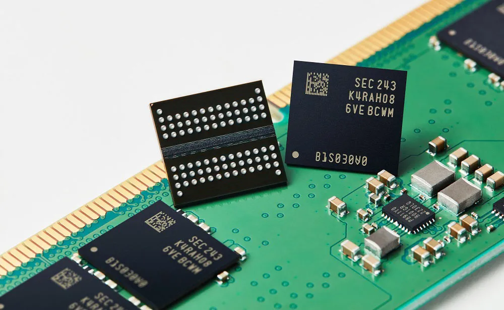
Just as they do for logic chips, memory makers must utilize new process technologies , to improve the performance, power, and area (PPA) of new DRAM device. Virtually all major steps in performance, capacity, and costs of DRAM are driven by new process nodes. For example, Samsung's 14nm (D1α) DRAM technology, featuring up to five EUV layers, enabled the company to build the world's first 24 Gb DDR5-7200 memory device in late 2021, ahead of the industry.

The leading memory makers — Micron, Samsung, and SK hynix — have developed multiple generations of 10nm-class fabrication processes, starting from 17nm – 19nm in the mid-2010s and all the way to ~12nm today. Now, Micron and SK hynix have introduced (1, 2) their 6th Generation 10nm-class process technologies — the so-called 1γ (1-gamma) or 1c nodes, and have even begun shipping actual products based on this node.
By contrast, Samsung seems a little behind with its 1γ/1c process, which will have an impact on its actual product roadmap. But keep in mind that Samsung's D1β (5th Gen 10nm-class) has a feature size of 12.5nm, which is smaller than its closest competitors. Micron's G5 10nm node sports a 13nm feature size, whereas SK hynix's 5th Gen 10nm-class node offers a feature size of 12.65nm, according to TechInsights.
The 1γ/1c process technology is an important node for all DRAM makers, as it's primed for use in the creation of high-capacity, high-performance DDR5 DRAM, as well as HBM4, GDDR7, and LPDDR5X memory devices.
The next-generation 1δ/1d production node will likely be even more important, however, as it will be the last 10nm-class node that will rely on the 6F2 cell design, which has been used for over a decade.
We anticipate that the new 4F2 cell structure for sub-10nm nodes will replace 6F2. The 1δ/1d process technologies are also expected to be introduced in the second half of 2026, though their ramp times remain to be seen. But this will be a real DRAM breakthrough, which will come to market toward the end of the decade, alongside the sub-10nm manufacturing processes.
The first sub-10nm production nodes are expected to arrive in late 2027 – 2028 at the earliest, with Samsung potentially leaping ahead of its rivals, according to TechInsights.
DDR5-10,000 modules are around the corner, DDR5-10,700 are next
In 2024, JEDEC released an updated version of its JESC79-JC5 specification, which defines DDR5 technology, and it officially extends DDR5 support to 8800 MT/s, as well as adding features like improved I/O training through Self-Refresh Exit Clock Sync.

This update reflects consensus among major memory and controller developers that DDR5-8800 is technically and economically feasible. The spec also defines the timings of CL62 for premium chips and CL78 for lower-grade ones, maintaining an absolute latency around 14ns despite higher CAS latency.
Traditionally, JEDEC specifications are extremely conservative, so Micron envisions that its DDR5 DRAMs made using its 1γ/1c fabrication process will hit data transfer rates of up to 9200 MT/s. SK hynix is also prepping 9200 MT/s memory devices with capacities up to 32 Gb, thus bringing together performance and capacity. However, speed bins beyond 9200 MT/s are not officially listed by anyone, to our knowledge.
Such DDR5-9200 32 Gb ICs are projected to hit the market relatively soon, then leading makers of enthusiast-grade memory modules will extract additional performance from such devices. You should expect high-performance 32 GB modules from the usual suspects — think Corsair, G.Skill, and V-Color — to hit 9600 MT/s on higher-end motherboards.

Intel is working hard to improve memory performance on its platforms, so industry insiders expect DDR5-10,000 modules to arrive with Intel's Arrow Lake-S Refresh CPUs early next year, with DDR5-10700 to follow later on.
We expect that some of these ultra-high-performance DDR5 modules will be CUDIMMs, equipped with a clock driver (CKD). The CKD regenerates the clock signal, which drives the actual memory chips, ensuring signal integrity and thus achieving stability and reliability at high data transfer rates.
For now, CUDIMMs are only officially supported by Intel platforms. But AMD is expected to introduce CUDIMM and then CSODIMM (SODIMM with a CKD) support sometime in 2026, likely beginning with Granite Ridge Refresh with speeds up to 10,000 MT/s, and then extending to next-generation CPUs based on the Zen 6 microarchitecture (e.g., Medusa Point) with speeds up to 10,700 MT/s or higher. Keep in mind that the information is strictly unofficial at this point.
Even before the CUDIMM support arrives, AMD plans to offer an enhancement that will enable high data transfer rates and low latencies on its consumer platforms, according to sources familiar with the topic. For now, the company is considering targets in the range of DDR5-6400 at CL26, which will reduce absolute latency to 8ns —a feat unprecedented even for enthusiast-grade DDR5.
32 Gb, 48 Gb, and 64 Gb DDR5 ICs
As we noted earlier in this article, new production technologies enable DRAM makers not only to boost performance or lower power consumption of their chips, but also to increase the capacity of their memory ICs. This will continue toward even 64 Gb DDR5 ICs.
The DDR5 specification and 1α/1a process technologies enabled DRAM producers to build 24 Gb DDR5 devices, enabling 24 GB, 48 GB, and 96 GB memory modules for client and server applications. With 1β/1b and 1γ/1c production nodes, we're looking at 32 Gb DDR5 ICs, which let memory module makers build unbuffered DIMMs and CUDIMMs with 64 GB, 128 GB (Micron is currently offering DDR5-8000 RDIMMs, for example), or even 256 GB capacities.
Currently, there are no confirmed plans for 48Gb or 64Gb DDR5 ICs with a definitive launch window, which suggests that they are still in the early planning stages. However, according to TechInsights, memory makers are seeking to achieve 48 Gb ICs, based on 1δ/1d process technologies sometime in 2027 – 2028.
As for 64 Gb DDR5 devices — the apex of DDR5 development — they will likely be reserved primarily for high-capacity data center-grade applications arriving from 2030 and onwards. Such ICs will likely be made using sub-10nm production nodes — think 0x (1st Gen) or even 0y (2nd Gen) and will therefore adopt 4F2 cell structures.
MRDIMMs
Speaking of data center applications, we cannot avoid mentioning multiplexed rank dual inline memory modules (MRDIMMs), which have been developed to overcome the bandwidth limitations of traditional RDIMMs. MRDIMMs run two DDR memory ranks in multiplexed mode, using a multiplexing registered clock driver (MRCD) chip for simultaneous rank access and 10 multiplexing data buffer (MDB) chips for data multiplexing. This setup enables supporting CPUs to communicate with MRDIMMs at an 8800 MT/s data transfer rate, while the memory chips operate at half speed to reduce latency and power use.

Intel's Xeon 6 platform is the first processor to support MRDIMMs, and the CPUs can work with the 1st-generation MRDIMMs at a data transfer rate of 8800 MT/s. However, not all Xeon 6-based servers use MRDIMMs, which is to be expected from a new technology.
The industry is now working on 2nd Generation MRDIMMs with capacities of 256 GB and above, as well as speeds of 12,800 MT/s. Such modules will be supported by AMD's EPYC 'Venice' and presumably 'Verano' CPUs in 2026 and 2027, respectively, as well as Intel's Xeon 'Diamond Rapids' and 'Coral Rapids' processors due in the second half of this decade. Each 2nd Gen MRDIMM will support a bandwidth of 102.4 GB/s, so a CPU with 16 memory channels will feature a peak bandwidth of 1.6 TB/s.
We have no indications whether there will be a 3rd Generation MRDIMM, but don't be too surprised if there is. Just keep in mind that DDR5 has a lot of headroom, with up to 8800 MT/s for memory devices, and therefore up to 17,600 MT/s in multiplexed mode — all within the latest specification.
DDR5 remains dominant
DDR5 memory continues to evolve with higher data transfer rates and higher capacities thanks to advanced process nodes like 1γ/1c and upcoming 1δ/1d, pushing DRAM ICs all the way to 9200 MT/s and enabling enthusiast-class memory modules with DDR5-10,000 or even DDR5-10,700 speed bins with appropriate CPUs.
As DDR6 is unlikely to arrive before 2029 – 2030, DDR5 will remain dominant, with ultra-fast CUDIMMs for client PCs and high-bandwidth MRDIMMs supporting next-gen platforms from AMD and Intel. With MRDIMMs, in particular, next-generation data center bandwidth is already reaching 8800 MT/s, with 2nd Gen versions targeting 12,800 MT/s in the second half of the decade.
