Intel Shows Off Multi-Chiplet Sapphire Rapids CPU with HBM

Intel
(Image credit: Tom Wassick/@wassickt)

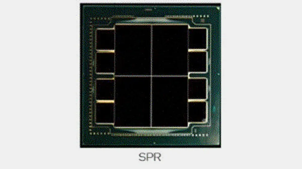
Intel formally confirmed that select 4th Generation Xeon Scalable 'Sapphire Rapids' processors will feature on-package HBM memory late last year, but the company has never demonstrated an actual CPU equipped with HBM or revealed its DRAM configuration. At the International Symposium on Microelectronics hosted by IMAPS earlier this week, the company finally showcased the processor with HBM and confirmed its multi-chiplet design.

While Intel confirmed on numerous occasions that Sapphire Rapids processors will support HBM (presumably HBM2E) and DDR5 memory and will be able to use HBM either with or without main DDR5 memory, it never showcased an actual HBM-equipped CPU, until this week (thanks to the picture published by Tom Wassick/@wassickt).

As it turns out, each of four Sapphire Rapids chiplets has two HBM memory stacks that use two 1024-bit interfaces (i.e., a 2048-bit memory bus). Formally, JEDEC’s HBM2E specification tops at a 3.2 GT/s data transfer rate, but last year SK Hynix started to mass-produce 16GB 1024-pin known-good stacked dies (KGSDs) rated for a 3.6 GT/s operation. 

If Intel opts to use such KGSDs, HBM2E memory will provide Sapphire Rapids CPU a whopping 3.68 TB/s peak memory bandwidth (or 921.6 GB/s per die), but only for 128GB of memory.  By contrast, SPR's eight DDR5-4800 memory channels supporting one module per channel and offering 307.2 GB/s will support at least 4TB of memory using Samsung's recently announced 512GB DDR5 RDIMM modules.

It is also noteworthy the HBM-equipped Sapphire Rapids comes in a large BGA form-factor and will be soldered directly to the motherboard. This is not particularly surprising as Intel's LGA4677 form-factor is pretty narrow and the CPU does not have enough space on its package for HBM stacks. 

Furthermore, processors that require a very high-performance memory subsystem like HBM tend to feature loads of cores that work at high clocks and feature a very high TDP. Keeping in mind that HBM stacks are also power-hungry, it may not be easy to develop a socket that would feed an HBM-equipped beast. Therefore, it looks like HBM-equipped SPRs will only be offered to select clients (just like Intel's Xeon Scalable 9200 CPUs with up to 56 cores) and will mostly be aimed at supercomputers. 

Another thing to note is that the shape of the SPR chiplets on the image are rectangular rather than square (as on early images of Sapphire Rapids in LGA4677 packaging). The author of the image said that it comes from an Intel chart "given by an Intel employee and labeled SPR, and verbally noted as Sapphire Rapids." That said, it looks like HBM-supporting Sapphire Rapids CPU might have a different chiplet configuration than regular SPR processors (at the end of the day, regular Xeon Scalable CPUs do not need an HBM interface that takes die space).

Intel's Sapphire Rapids processors will feature a host of new technologies, including PCIe Gen 5 support with CXL 1.1 protocol for accelerators on top, a hybrid memory subsystem supporting DDR5 and HBM, Intel’s Advanced Matrix Extensions (AMX) as well as AVX512_BF16 and AVX512_VP2INTERSECT instructions designed for datacenter and supercomputer workloads, and Intel's Data Streaming Accelerator (DSA) technology, just to name a few.

Earlier this year we learned that Intel's Sapphire Rapids uses a a multi-chip package with EMIB interconnects between the die, unlike its predecessors that are monolithic. While the number of cores is something that depends on yield and power (some reports indicate that SPR will feature up to 56 active cores, but the actual chiplets may carry as many as 80 cores), it is evident that the 4th Generation Xeon Scalable will be the first to use Intel's latest packaging technologies and design paradigm.


Anton Shilov
Freelance News Writer

Anton Shilov is a Freelance News Writer at Tom’s Hardware US. Over the past couple of decades, he has covered everything from CPUs and GPUs to supercomputers and from modern process technologies and latest fab tools to high-tech industry trends.

  • MB007
    "Therefore, it looks like HBM-equipped SPRs will only be offered to select
    clients (just like Intel's Xeon Scalable 9200 CPUs with up to 56 cores) and will mostly be aimed at supercomputers. "

    The question is who would be willing enough to integrate those in its supercomputers anymore, after the fiasco with Aurora. Which is still a running fiasco...
    Reply
  • mitch074
    Pfeh! It's all a bunch of cores glued together, no way it's real technological innovation...
    Reply
  • JayNor
    MB007 said:

    The question is who would be willing enough to integrate those in its supercomputers anymore, after the fiasco with Aurora. Which is still a running fiasco...

    Intel already said that Aurora is using these.
    Reply
  • MB007
    You did not really get my point. Of course Aurora is supposed to use these. But Intel practically broke multiple contract agreements, they were not able to hold any time line of whatsoever. Its still not finished, after dozens of frign years. In the end Aurora was a very expensive prestige project for intel, that pretty much back fired. They did not really make a single dime with it, on the contrary charges were in the hundreds of millions. And even worse, they simply lost quite some credibility with it. So I ask you again, who is willing to take the risk.
    Reply
  • JayNor
    I think the SPR chips have been sampling since last Nov.. ... pcie5, cxl, ddr5, gen3 optane, DSA, AMX matrix math on bfloat16... and 8 stacks of HBM. Pretty amazing if it all works.

    6x 9k units of Ponte Vecchio GPUs may be the hold-up now. Who else is doing 47 tile GPUs?

    Maybe we'll see a demo in a couple of weeks.
    Reply
  • Integr8d
    mitch074 said:
    Pfeh! It's all a bunch of cores glued together, no way it's real technological innovation...

    The stock market said otherwise;)
    Reply
  • JayNor
    BSC seems happy with Optane, so Intel is solving some problems that others haven't.
    Reply
  • JayNor
    The hbm is not so much of an innovation, but we haven't heard the whole story yet. One of the diagrams I saw shows 4 lanes of slingshot going directly into each SPR. They also haven't announced how they are using the DSA.

    https://ecpannualmeeting.com/assets/overview/sessions/SYCL_Programming_Model_for_Aurora.pdf
    Intel also hasn't shown their Rambo Cache details yet. I saw an Intel patent app with the whole foveros base layer of a GPU populated with a grid of SRAM chiplets, so Intel has some show-and-tell coming.
    Reply
  • TerryLaze
    MB007 said:
    You did not really get my point. Of course Aurora is supposed to use these. But Intel practically broke multiple contract agreements, they were not able to hold any time line of whatsoever. Its still not finished, after dozens of frign years. In the end Aurora was a very expensive prestige project for intel, that pretty much back fired. They did not really make a single dime with it, on the contrary charges were in the hundreds of millions. And even worse, they simply lost quite some credibility with it. So I ask you again, who is willing to take the risk.
    Maybe they did not make a single dime with it specifically, but if they used the wafers that where to be used for aurora to supply the mobile and desktop market in the last two years then they made a crap ton of money from it even with the fines.

    And they also gained a lot of credibility with OEMs and "the common man" by being able to supply the whole market as if nothing had happened and without increasing the prices at all or reducing the value.

    Having a business is all about weighing the pros and cons of everything and going with what you believe will benefit your company the most.
    Reply
  • MB007
    jeez its like talking against a wall. How did you come up with this fairy tell.
    One of their big problems was with their process node, yields were crappy as it only can get. So those wafers werent reallocated for other purposes.
    And dont talk like they were able to supply, because clearly the last ERs showed more or less, growth was catastrophic considering we were and still are in a mega semi conductor cycle.
    So supply is one thing, but apparently the demand for their products was not the same, because everybody else benefited much more from the cycle than intel was able to, although they were less capacity strained. think about that rather.
    Reply