Lasers Enable Finer Chip Structures, Advance of Moore's Law
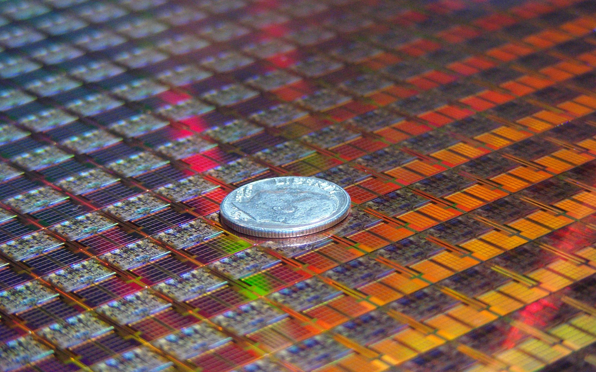
A research team at the Massachusetts Institute of Technology (MIT) said it has found a new way to shrink circuit structures in semiconductors.
Get Tom's Hardware's best news and in-depth reviews, straight to your inbox.
You are now subscribed
Your newsletter sign-up was successful
Current chip manufacturing relies on photolithography techniques, which can only produce chip features that are larger than the wavelength of the light applied.
A process that is described in the paper "Breaking the Far-Field Diffraction Limit in Optical Nanopatterning via Repeated Photochemical and Electrochemical Transitions in Photochromic Molecules", published in Physical Review Letters, can create complex structures chip structures 1/8 the size of the wavelength of the light used. According to the researchers, an effect called stimulated emission depletion imaging (STED) enabled them to go beyond the current limitations of photolithography. In STED, scientists leverage the fluorescent characteristics of materials to emit light when targeted by a laser beam. By controlling the laser's power, the researchers can affect the strength of light emitted and, if the power falls enough, cause a "dark patch" that is smaller than the wavelength of the laser light itself. These dark patches can be used as masks, which can be applied to a surface.
The MIT researchers believe that their invention could be used to create semiconductors with much finer structures than possible today. There could also be an opportunity to apply this technology in photonic devices, MIT said.
Article continues belowGet Tom's Hardware's best news and in-depth reviews, straight to your inbox.

Douglas Perry was a freelance writer for Tom's Hardware covering semiconductors, storage technology, quantum computing, and processor power delivery. He has authored several books and is currently an editor for The Oregonian/OregonLive.
-
amk-aka-Phantom theuniquegamerThat means we can get 32 or more cores in the mobile chips in next few years.Reply
... and over 9000 in the desktop ones :D
Remember, whatever "mobile" has to offer, desktop will always pwn it. -
guru_urug Combine this with the molybdenite tech in the previous article and we have pocket supercomputers. Seriously the future is really exciting!!! Cant waitReply -
amk-aka-Phantom Reply9336275 said:Now THAT deserves a patent, not some buttons on scren.
No way. You're again patenting an IDEA, FFS! That will just slow the implementation down! Where would the humanity be if everyone would be patenting everything from the invention of the wheel, huh? -
salgado18 Reply
That's real technology, a new process of production of really small circuits. It takes years of research, a lot of knowledge and study, and a hell lot of money to even make it right, so it definitely deserves a patent to these guys.9336276 said:No way. You're again patenting an IDEA, FFS! That will just slow the implementation down! Where would the humanity be if everyone would be patenting everything from the invention of the wheel, huh?
If that's not a patent, then what is? -
mildgamer001 amk-aka-Phantom... and over 9000 in the desktop ones Remember, whatever "mobile" has to offer, desktop will always pwn it.Reply
ITS OVER 9000!!!!
