Despite Massive Investments, Samsung Chip Businesses Seem to Falter
Money does not always matter?

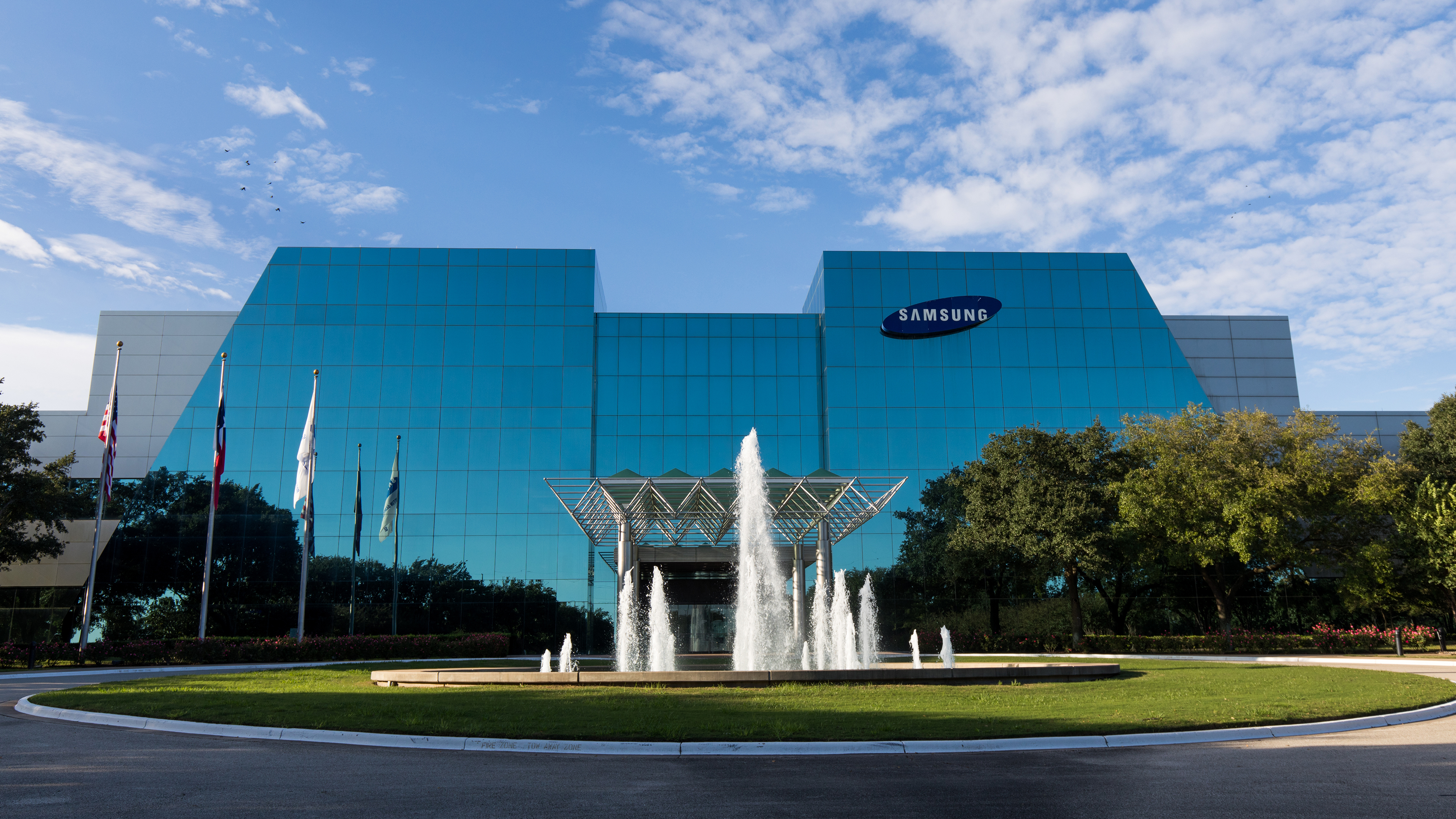
Being one of South Korea's largest vertically integrated chaebols (a large industrial conglomerate ran and controlled by an individual or family in South Korea), Samsung can invest more money in its semiconductor business that almost any other company and adopt leading process technologies ahead of everyone else. But that doesn't mean that Samsung is a technology leader in producing logic chips or memory. In fact, it is lagging behind TSMC, Intel, and Micron when it comes to performance and cost.
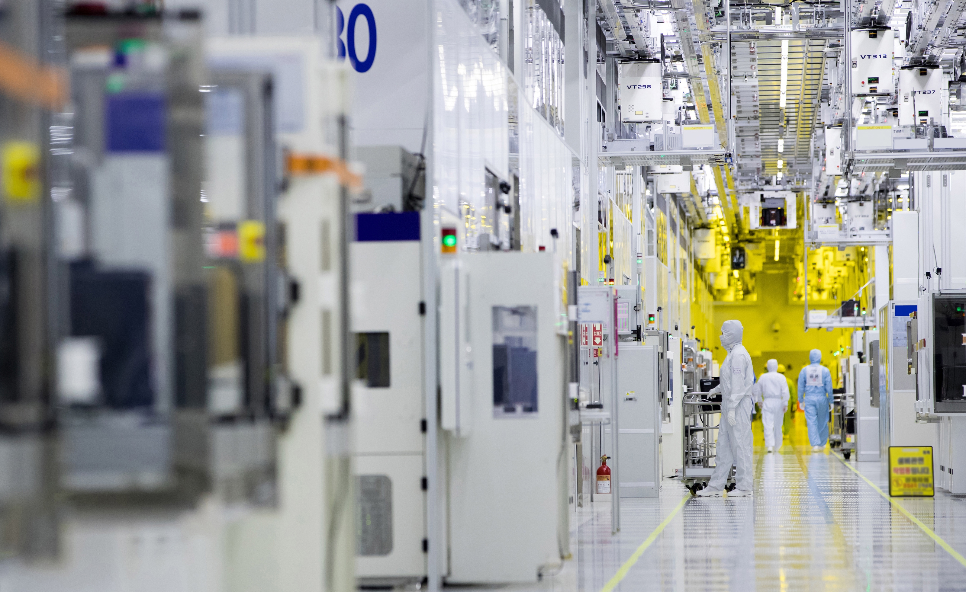
Samsung spent $93.2 billion on expanding its semiconductor production capacity for its memory and foundry divisions over the 2017–2020 period, more than Intel and TSMC invested. In addition, the company spent billions on researching and developing new process technologies. Because of extreme spending, Samsung Foundry and Samsung Semiconductor were the first to adopt extreme ultraviolet (EUV) lithography for logic production in 2018 and DRAM production in 2021.
But using the latest lithography tools doesn't mean that the company's foundry, memory, and chip development businesses are guaranteed to thrive. In fact, a Samsung DRAM engineer said is a blog post that the company's controversial corporate culture might be a reason why its semiconductor businesses have faced troubles in recent years, reports DigiTimes.
Foundry Nodes
EUV lithography is meant to reduce multi-patterning, increase yields, decrease cycle times, while ultimately increasing performance and lowering costs. But Samsung Foundry has failed to get many additional customers with its 7LPP, 5LPE, and 5LPP fabrication technologies. The company's only big EUV win was landing orders from Qualcomm. By contrast, Nvidia only used Samsung's 8LPP node, a highly advanced 10nm-class technology that only uses deep ultraviolet (DUV) lithography.
In the past year or so rumors emerged that Samsung's 4nm yields were low and the node had not quite lived up to expectations. Like other contract makers of semiconductors, Samsung Foundry does not comment on yields, to some degree because they are its trade secrets for itself and its customers. When Qualcomm moved production of its Snapdragon 8 Gen 1 SoC from Samsung Foundry's 4nm-class technology (4LPE or 4LPP) to one of TSMC's N4 nodes, it could increase its clocks and at the same time cut its power consumption (i.e., significantly increase performance per watt), which demonstrates that 4LPE/4LPP is significantly less competitive than its direct rival at least from performance per watt point of view. One thing to keep in mind here is that Samsung Foundry's 4nm family of manufacturing processes are the company's third generation EUV node and based on the fact that it is behind a competing technology, we can draw some unfavorable conclusions about actual capabilities of Samsung's 7LPP, 5LPE, and 5LPP.
One of a few indirect confirmations about insufficient leading-edge yields at Samsung Foundry was revealed back in April, when Samsung's LSI division marketing chief pre-announced yield improvements for flagship SoCs.
"In the second quarter, we expect our SoC supply to grow significantly led by yield improvements for flagship SoCs and the addition of mid-range products to our lineup," said Kenny Han (via Seeking Alpha).
Get Tom's Hardware's best news and in-depth reviews, straight to your inbox.
In recent weeks there have been rumors that yields of chips made using Samsung Foundry's 3GAE node (3nm-class, gate-all-around transistors, early) did not meet expectations too, but considering that the company's 'early' nodes are usually used almost exclusively by the firm's LSI division and the latter barely shares all the details with third parties, we have no idea how to verify the rumors even unofficially. Officially, Samsung only says that it had implemented a new flow to speed up time-to-yield starting from its 3nm-class nodes.
“We have improved the node development system from 3nm,” a representative for Samsung said. “We actually now have a verification for each stage of development. This will help us reduce the yield ramp-up period later on, improve our profitability and also ensure a stabler supply.”
Given that semiconductor companies are skilled in keeping their secrets (and Samsung is probably more secretive than many others), we can only wonder about the reasons behind Samsung Foundry's allegedly poor yields. Typically, companies fail when they set themselves too ambitious or too mediocre goals. With Samsung Foundry's 7nm and more advanced nodes, the company made a bet on usage of EUV and to deploy it in 2018 it had to introduce a number of proprietary technologies and production methods (e.g., as not using pellicles on photomasks, which might have an impact on yields).
By contrast, TSMC did not use EUV tools for its N7 node in 2018 and only offered EUV layers with its subsequent N7+ technology in 2019 after hiccups of the original process have either been solved or at least identified as well as when EUV tools matured. TSMC is known for its rather conservative approach to process technology development as well as usage of new tools, which provides a lot of predictability to its customers. Predictable advantages (even if they are not dramatic) along with predictably high yields are perhaps the reasons why TSMC has landed orders from technology giants like Apple and AMD that have different tactics when it comes to adoption of new process technologies.
DRAM Nodes
But Samsung's foundry division was not the only business unit to put big bets on EUV. Samsung Semiconductor shipped the first test DRAM chips made on its D1x, an EUV-enhanced process, to its customers in early 2020, but the technology has not been used for high-volume manufacturing. Instead, Samsung's DRAM business unit started to ship memory chips made using its D1a node (which uses EUV tools for five layers) in late October, 2021.
Samsung's D1a is the company's 4th Generation 10nm-class DRAM node, also known as 13nm. Development of this node took the company quite a while, leaving it behind both Micron (which started shipping 1a-based DRAM ICs in June, 2021) and SK Hynix (which initiated production of 1a DRAMs in July, 2021).
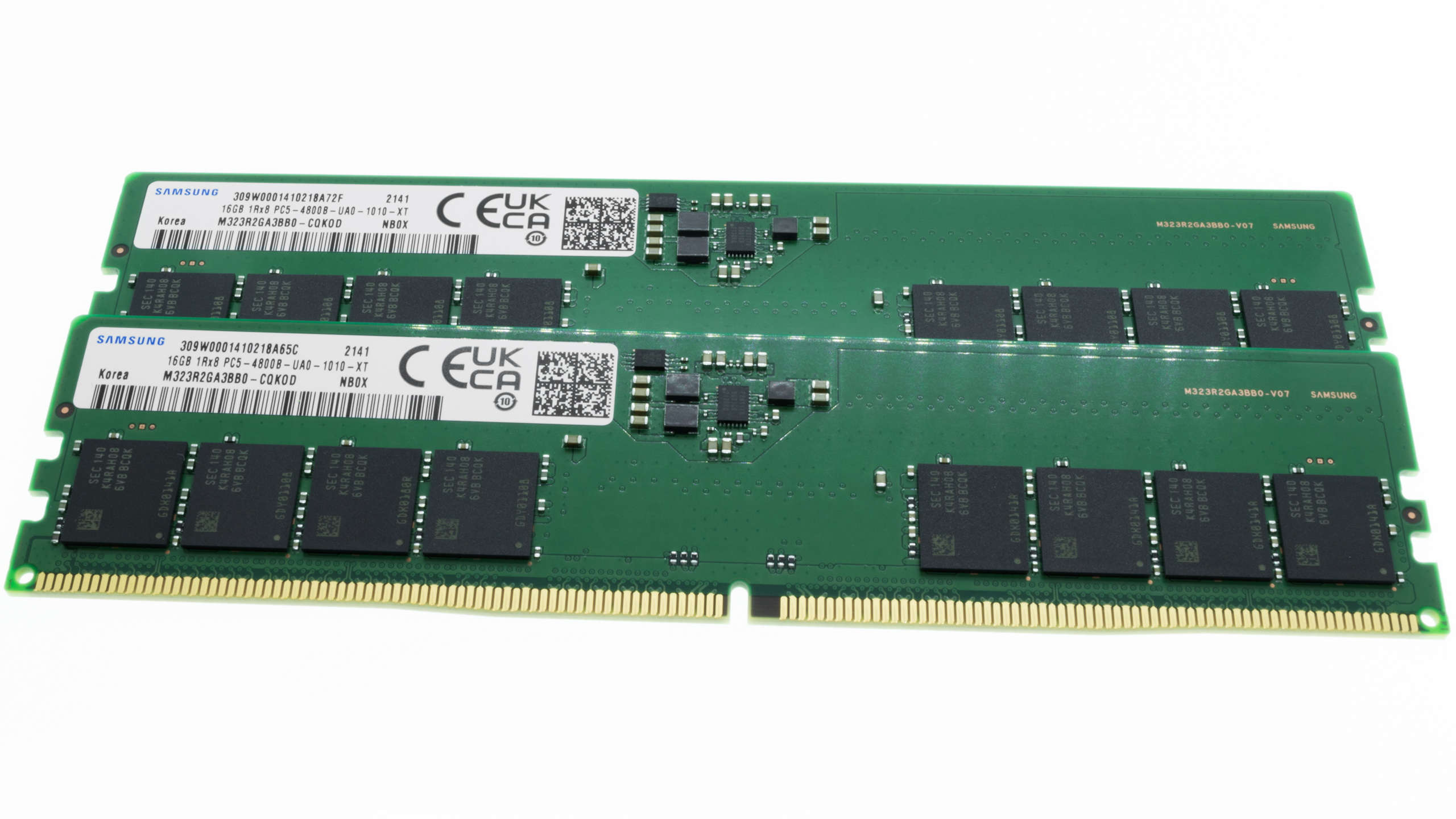
Micron intends to use its 1a fabrication technology (which does not use EUV at all) for all types of DRAM it ships and has already widely deployed this node, according to media reports. As a result, Micron not only beaten Samsung to punch with its 1a process, but also left it behind with the pace of its adoption. As a result, Micron's memory is cheaper to make, which is particularly beneficial when it comes to DDR5 ICs that are physically larger than DDR4 chips of the same capacity and produced on the same node.
Over time, Samsung may regain leadership because of its extensive experience with EUV-based DRAM process technologies, but for now the company does not seem to be leading the game. Interestingly, Micron sees usage of EUV tools as a disadvantage because of EUV scanner costs, limited productivity of EUV equipment, imperfect critical dimension (CD) uniformity, and longer cycle times.
In a bid to leapfrog the competition, Samsung intend to skip 1b process technology and refocus to 1c (11nm) instead, according to the DigiTimes report that cites the engineer. This information was denied in April, but plans tend to change.
"I think it is fair to say that our 12nm development plan is being carried out stably, and the subsequent nodes would also be developed according to our mid- to long-term technology roadmap," a representative for Samsung said.
LSI Business
But Samsung has an advantage over Micron, SK Hynix, and TSMC. It sells much more than memory chips and semiconductor manufacturing services. It sells all kinds of consumer electronics, including smartphones that cost over $1,000 per unit or televisions that cost significantly more. Therefore, even if its yields are not as high and its costs are not as low, Samsung still remains profitable.
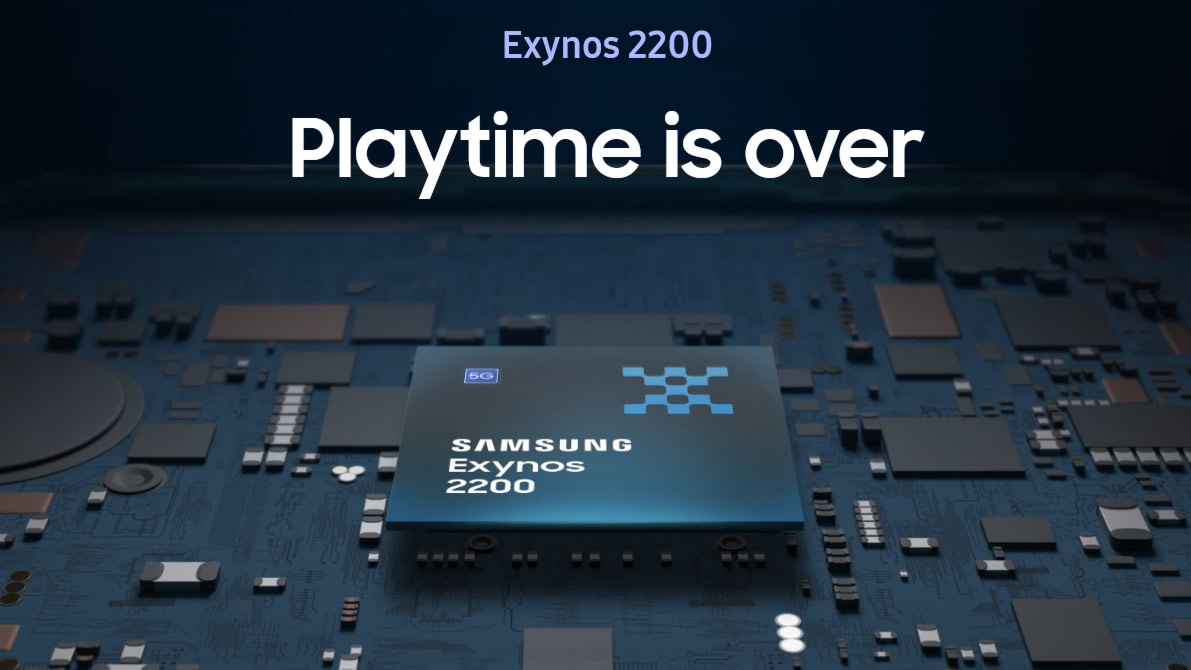
But the problem with mediocre nodes and yields is that they affect the performance and capabilities of Samsung's own system-on-chips (SoCs), which may fail to meet expectations. This is what happened with the Exynos 2200, which wasn't faster than Qualcomm's Snadragon 8 Gen 1 made using the same process technology.
Summary
While Samsung can spend fortunes on its semiconductor businesses, this doesn't guarantee its success. In the past couple of years, we have seen various direct and indirect evidence that the company's semiconductor businesses are struggling. Samsung Foundry's contract manufacturing business is not growing as fast as that of its rivals, whereas its nodes are falling short of expectations. Samsung Semiconductor was several months behind its rivals with its 1a DRAM fabrication process, whereas the performance of Samsung's LSI flagship SoCs is lower compared to its competitors.
Like other huge companies, Samsung is very durable and has enough financial, intellectual, and technological resources to survive plenty of challenges. The only problem is when this happens and whether the current management of the company is up to the task.

Anton Shilov is a contributing writer at Tom’s Hardware. Over the past couple of decades, he has covered everything from CPUs and GPUs to supercomputers and from modern process technologies and latest fab tools to high-tech industry trends.
-
KananX The issue is that Samsung is built around a philosophy of pure performance at all costs. Their infamous former CEO having a rage at his employees, is unforgettable. This isn’t the best philosophy to have in a company, modern companies should provide a culture of creativity, and this will only happen if the character of the company is positive, not centered around performance performance.Reply -
dalek1234 ReplyKananX said:The issue is that Samsung is built around a philosophy of pure performance at all costs. ...
I would go a bit further and also quote Korean work colture as another fac tor to blame. An employee working for a Korean company is to have all his/her blood/sweat/tear squeezed out of. Korean companies around the globe aren't much better either. That's not an environment where employees inovate. it's an environment few notches below a Gulag. -
KananX Reply
It’s very hard yes but also typically East Asian. The key is to have some semblance of balance to this at least, which doesn’t seem to be the case at Samsung, at least not their foundry business. Many Asian companies do better in this regard.dalek1234 said:I would go a bit further and also quote Korean work colture as another fac tor to blame. An employee working for a Korean company is to have all his/her blood/sweat/tear squeezed out of. Korean companies around the globe aren't much better either. That's not an environment where employees inovate. it's an environment few notches below a Gulag. -
dalek1234 ReplyKananX said:It’s very hard yes but also typically East Asian. The key is to have some semblance of balance to this at least, which doesn’t seem to be the case at Samsung, at least not their foundry business. Many Asian companies do better in this regard.
An anecdotal piece: A friend of mine had an upcoming interview with one of LG offices in Poland. He was concerned because of Korean companies reputation for treating their employees. So naturally he wasn't very exited, but needed a job so he went for the interview. He passed, they made him an financial offer. It was far below industry standard, so he walked about laughing (figuratively). -
KananX Reply
Interesting, I’m speculating a bit here, but I think they can afford things like this because of the abundance of talent they have in east Asia. Of course East Asians don’t have the creativity of westerners, but they perform and cost less, right.dalek1234 said:An anecdotal piece: A friend of mine had an upcoming interview with one of LG offices in Poland. He was concerned because of Korean companies reputation for treating their employees. So naturally he wasn't very exited, but needed a job so he went for the interview. He passed, they made him an financial offer. It was far below industry standard, so he walked about laughing (figuratively). -
isofilm Poor pitiful workers, if they had better work conditions and nicer management, their IQ would suddenly improve.Reply
Samsung Foundries primary problems are lack of intelligence, and a propensity to lie and obfuscate if all else fails.
Their fearless leader Comrade Lee Jae Yong (Vice Chairman) was just released from prison for embezzlement, bribery, and perjury.


