European Processor Initiative Receives First EPAC RISC-V Sample Chips for Testing
RISC-V is taking over the European computing landscape

Get Tom's Hardware's best news and in-depth reviews, straight to your inbox.
You are now subscribed
Your newsletter sign-up was successful
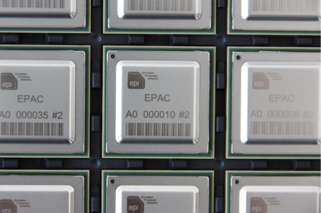
European Processor Initiative (EPI) has been working on providing independence for the European Union in the high-performance computing (HPC) field, by developing custom RISC-V-based accelerators. Called the European Processor Accelerator (EPAC) chip, designed for high efficiency and high throughput computation, it has been successfully taped out and is being tested at EPI's labs.
The European Processor Initiative started as a project of 28 partners from 10 European countries to equip the EU with custom processors and technologies that will enable the Union to become a technology-independent force focused on science and innovation. To achieve this, the project aims to build a completely custom HPC system, starting with custom processors. As the project notes: "One key segment of EPI activities is to develop and demonstrate fully European-grown processor IPs based on the RISC-V Instruction Set Architecture, providing power-efficient and high-throughput accelerator cores named EPAC (European Processor Accelerators)."
And today, the project has delivered its promises as the very first batch of chips are being tested in EPI's labs. The RISC-V processors are designs containing multiple special-purpose accelerators, all centered around the RSIC-V ISA and its design principles. The processor contains four tiles of Vector Processing Units (VPUs) made up from Avispado RISC-V core designed by SemiDynamics, and vector processing elements design by Barcelona Supercomputing Center and the University of Zagreb. In each tile, there are home nodes and L2 cache for cache systems, which are the contributions of Chalmers and FORTH. For additional acceleration, there are Stencil and Tensor accelerators (STX) engineered by Fraunhofer IIS, ITWM, and ETH Zürich, and the variable precision processor (VRP) deigned by CEA LIST.
For keeping all of these components connected, there is a high-speed Network-on-Chip (NoC) router and SERDES developed by EXTOLL. Other off-chip connections are unknown so far, however, we assume that there will be DDR5 and PCIe Gen4 or Gen5 I/O options to utilize.
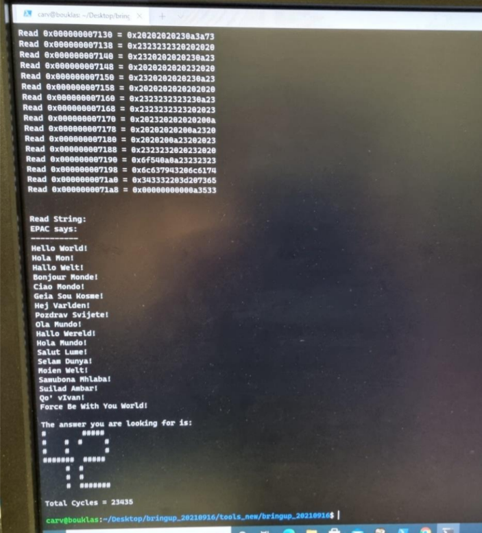
The chip has been taped out on GlobalFoundries 22nm FDX low-power semiconductor node that managed to pack the chip in a 26.97mm2 die area. The test package is type FCBGA with 22 x 22 solder balls in a grid array and the chip a target frequency of 1GHz, so far, as the final chip could have an aim for frequency target. In the image below, you can see the classic "Hello World" test being performed on the new platform.

The immediate outlook for this chip is continuous improvement, alongside the rest of the HPC IPs which still need to be designed, and once everything is ready, EPI plans to combine it into a powerful HPC system used for all kinds of workloads.
Get Tom's Hardware's best news and in-depth reviews, straight to your inbox.