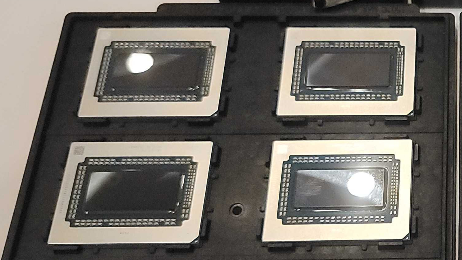
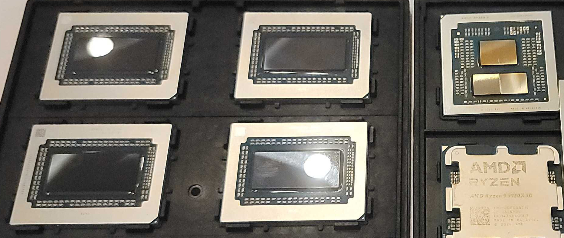
AMD's first RDNA 4 GPU die pictured: Navi 48 around 390 mm2, targeting mainstream gamers
Small and rectangular.

AMD's Navi 48 graphics processing unit, based on the RDNA 4 architecture that the company briefly demonstrated yesterday, is significantly smaller than its predecessors from the RDNA 3 generation. The small die size may be proof that the company does not intend to position its RDNA 4 GPUs to compete with Nvidia in the high-end market segment.
The die size of AMD's Navi 48 GPU, produced on TSMC's 4nm-class process technology, is around 390 mm², according to the calculations of blogger David Huang. The GPU is slightly larger than Nvidia's AD103, which is made on a similar process technology.
The Navi 48 graphics processor is monolithic and is not accompanied by any memory cache dies, unlike its Navi 31 and Navi 32 predecessors. This makes it impossible to make an apples-to-apples comparison between its die size and the die sizes of its predecessors. However, if we combine the sizes of Navi 3x graphics compute dies (made on N5) and memory cache dies (made on N6), we can estimate that Navi 32 uses around 346 mm² of silicon, whereas Navi 31 uses 529 mm² of silicon. These measurements roughly correspond to the positioning of the graphics processors in the performance mainstream and high-end segments, respectively. That said, it is safe to say that AMD did not aim to create an expensive GPU with its Navi 48.
TSMC's 4nm-class manufacturing technologies (e.g., N4P) belong to the same process development kit as the foundry's 5nm-class fabrication processes. These technologies provide about 1.06x higher transistor density, up to 11% higher performance (at the same power and transistor count), or up to 22% power reduction (at the same speed and transistor count). While N4P offers noticeable advantages over N5, do not expect a major performance improvement from adoption of a new node alone. Thus, any performance improvements in RDNA 4 or the Radeon RX 9070 XT over existing offerings are likely the result of architectural enhancements rather than the adoption of a new node.
In theory, AMD could adopt N4C for a higher transistor count at 390 mm² and/or up to 8.5% reduced costs. However, that would come at the cost of performance, making adoption of this node unlikely for a GPU.
When AMD first showcased the Navi 48 GPU yesterday, it was presented as the company's Hawk Point Refresh processor. However, it certainly resembled the Navi 48 GPU from AMD's press materials, not a Hawk Point CPU. We asked AMD for clarification, but the company declined to comment. As such, and when comparing to the company's other press materials, logic dictates this is in fact the first sighting of RDNA 4.
Get Tom's Hardware's best news and in-depth reviews, straight to your inbox.

Anton Shilov is a contributing writer at Tom’s Hardware. Over the past couple of decades, he has covered everything from CPUs and GPUs to supercomputers and from modern process technologies and latest fab tools to high-tech industry trends.
- Paul AlcornEditor-in-Chief
-
bit_user Reply
Good job to all involved!The article said:When AMD first showcased the Navi 48 GPU yesterday, it was presented as the company's Hawk Point Refresh processor. However, it certainly resembled the Navi 48 GPU from AMD's press materials, not a Hawk Point CPU. We asked AMD for clarification, but the company declined to comment.
I'd also point out that the die-to-die communication did impose some power overhead, on its predacessor. Going monolithic should improve efficiency, even if it's a little more wasteful to fab I/Os and cache on N4P than N6.
I never found an answer to the question of whether MCDs only cached their own memory bank or whether their caching domain was global. If the former, it could've resulted in it behaving like a much smaller cache, in some cases. If the latter, it would've compounded the inefficiency of the die-to-die communication. -
Pierce2623 Actually 7nm to 5nm still managed to maintain better SRAM scaling than 3nm did. Staying on-die for the L3 (excuse me, INFINITY CACHE) should be helpful for latency too.Reply -
bit_user Reply
In RDNA2, I got the sense that Infinity Cache was basically L2. I think you're right that RDNA3's MCDs are L3, though.Pierce2623 said:Staying on-die for the L3 (excuse me, INFINITY CACHE) should be helpful for latency too.
GPUs tend to be pretty resilient to latency. The main benefit of something like a L3 cache would be bandwidth. For instance, the RTX 4090 has only two levels of cache and its L2 latency is 138 ns, which is way more than the DDR5 latency in desktop CPUs!!
Source: https://chipsandcheese.com/p/microbenchmarking-nvidias-rtx-4090And keep in mind, those measurements were taken when the GPU was otherwise idle. So, those are best-case latency numbers!
BTW, AMD said it put the Tag RAM for its L3 on the GCD. I guess that would help with latency, but it might also answer the question of whether the caching domain for the L3 was global or tied to that MCD.
Edit: here's the latency data from two RDNA3 GPUs. Even with the RX 7900 XTX's chiplet architecture, latency doesn't seem worse than the RTX 4090.
Source: https://chipsandcheese.com/p/latency-testing-is-hard-rdna-3-power-saving?utm_source=publication-search -
Mama Changa Reply
Yeah even 5nm to 3nm was virtually zero scaling. However, it appears TSMC has had a breakthrough and 2nm will see the first tangible improvement in SRAM scaling since we went from 10nm to 7nm. Even 7nm to 5nm was not great.Pierce2623 said:Actually 7nm to 5nm still managed to maintain better SRAM scaling than 3nm did. Staying on-die for the L3 (excuse me, INFINITY CACHE) should be helpful for latency too. -
DS426 AMD does net back some perf and power efficiency by not having MCD's, so yep, I'm curious to see where the 9070 lands in terms of gen-on-gen gains and against nVidia in both raw perf terms and value (perf/$ if you will).Reply
Some waste as mentioned but also simpler packaging process, so it's probably more than made up in cost terms.
