AMD Radeon Vega Frontier Edition 16GB Review
Why you can trust Tom's Hardware
Vega Architecture & HBM2
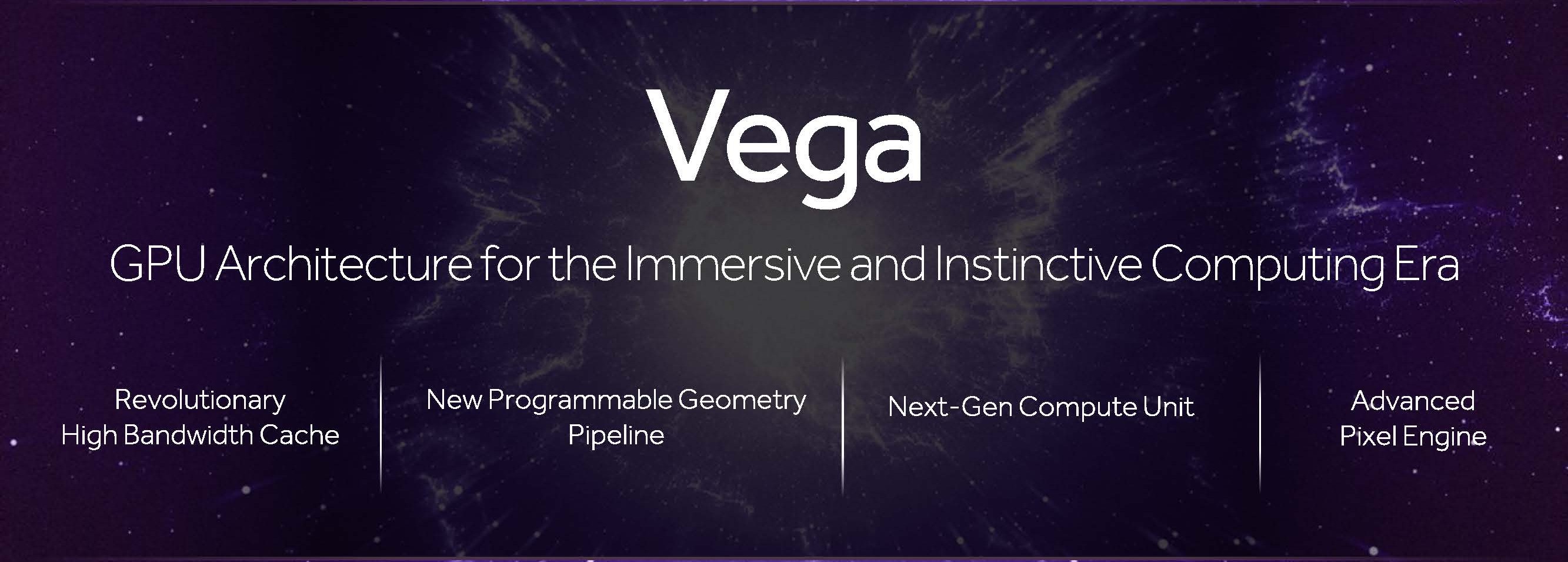
Vega represents a new GPU generation for AMD, with a reported >200 changes and improvements separating it from the implementation of GCN that came before.
HBM2: A Scalable Memory Architecture
Both AMD and Nvidia are working on ways to reduce host processor overhead, maximize throughput to feed the GPU, and circumvent existing bottlenecks—particularly those that surface in the face of voluminous datasets. Getting more capacity closer to the GPU in a fairly cost-effective manner seemed to be the Radeon Pro SSG’s purpose. And Vega appears to take this mission a step further with a more flexible memory hierarchy.
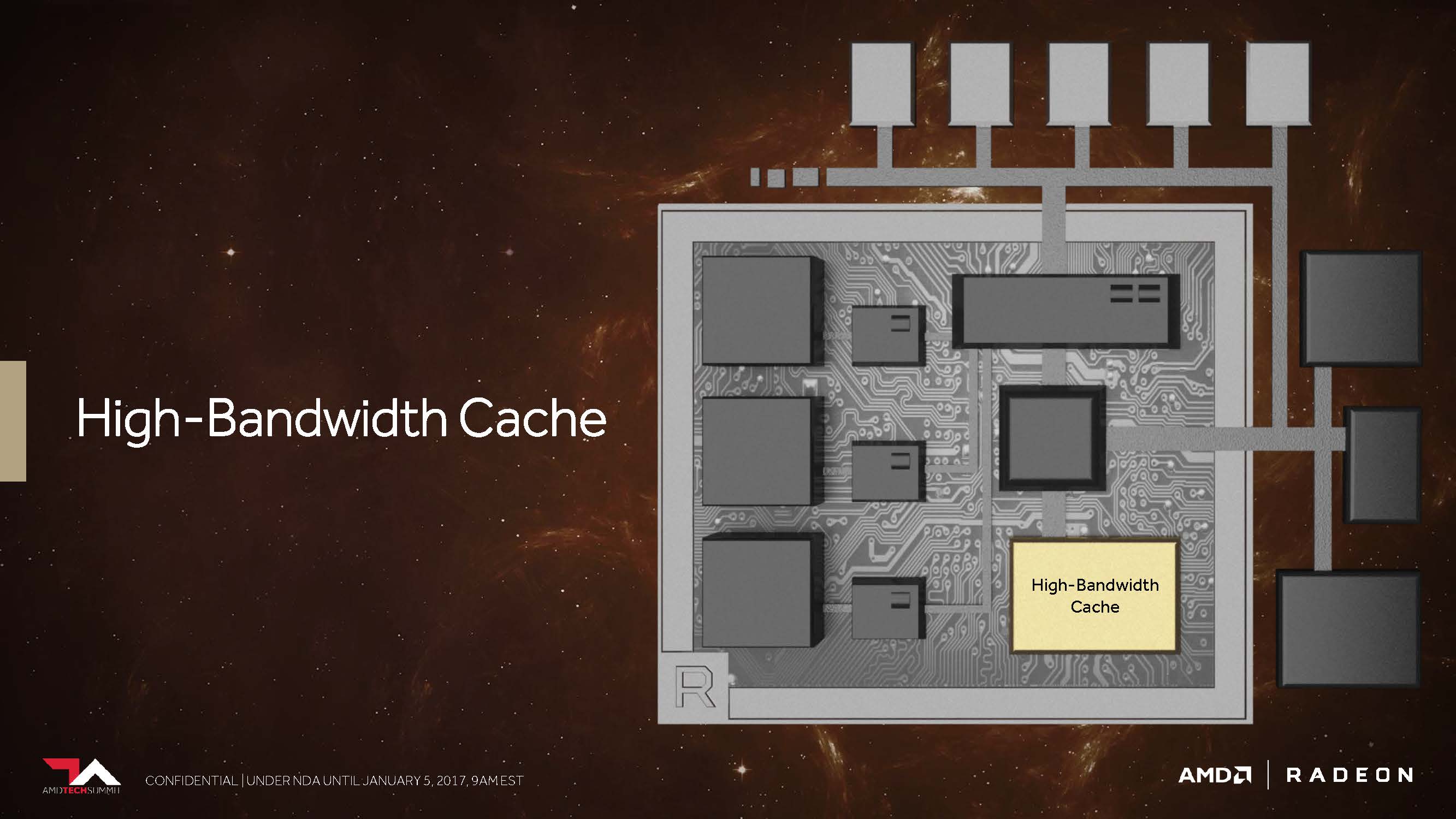
It’s no secret that Vega makes use of HBM 2; AMD officially introduced the memory technology to us more than six months ago. At the time, we also discovered that the company calls this pool of on-package memory—previously the frame buffer—a high-bandwidth cache. Got it? HBM2 equals high-bandwidth cache. Why? Because AMD says so.
No really, why? Well, according to Joe Macri, corporate fellow and product CTO, the vision for HBM was to have it be the highest-performance memory closest to the GPU. However, he also wanted system memory and storage available to the graphics processor, as well. In the context of this broader memory hierarchy, sure, it’s logical to envision HBM2 as a high-bandwidth cache relative to slower technologies. But for the sake of disambiguation, we’re going to continue calling HBM2 what it is.
After all, HBM2 in and of itself represents a significant step forward. An up-to-8x capacity increase per vertical stack, compared to first-gen HBM, addresses questions enthusiasts raised about Radeon R9 Fury X’s longevity. Further, a doubling of bandwidth per pin significantly increases potential throughput.
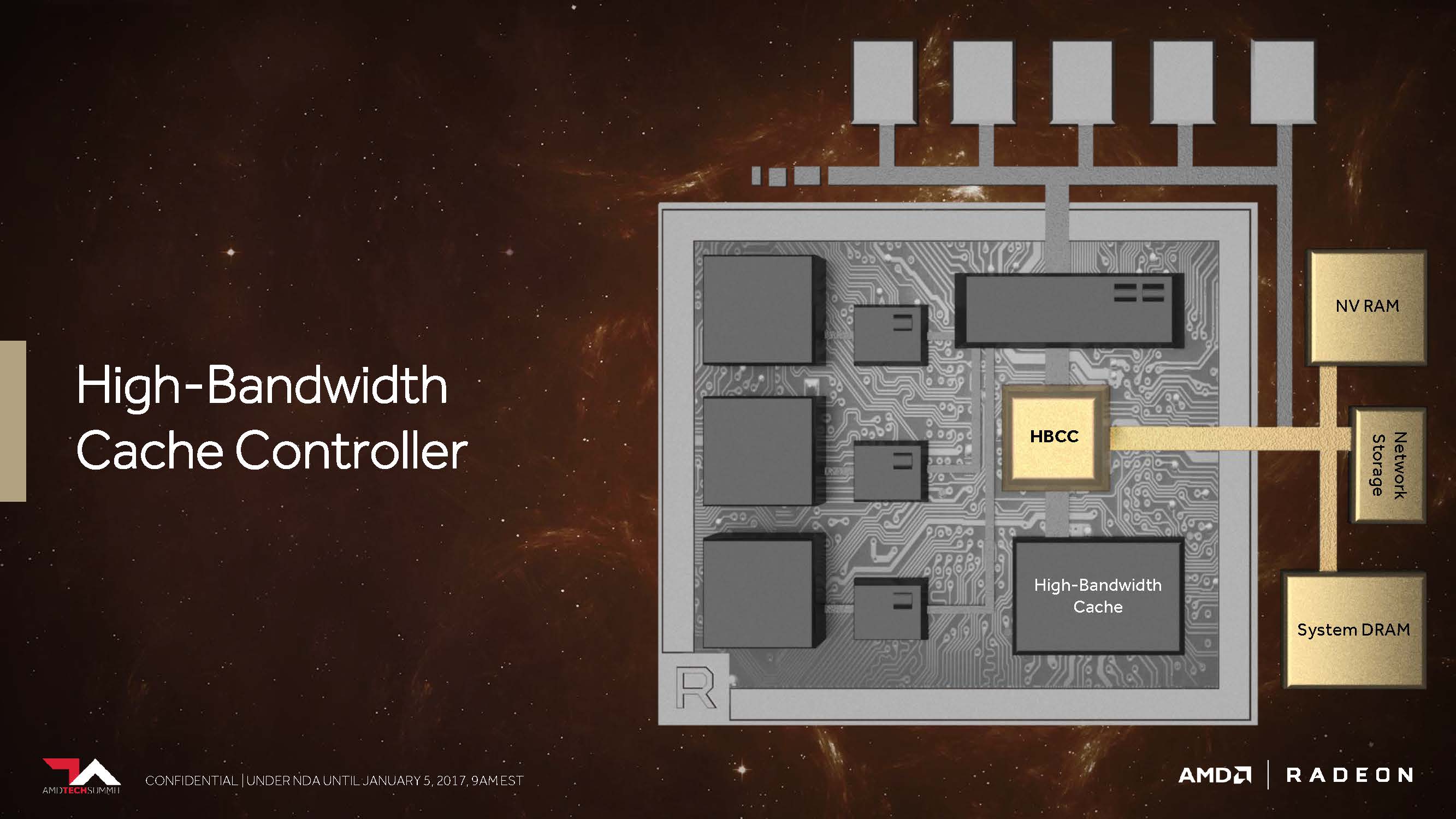
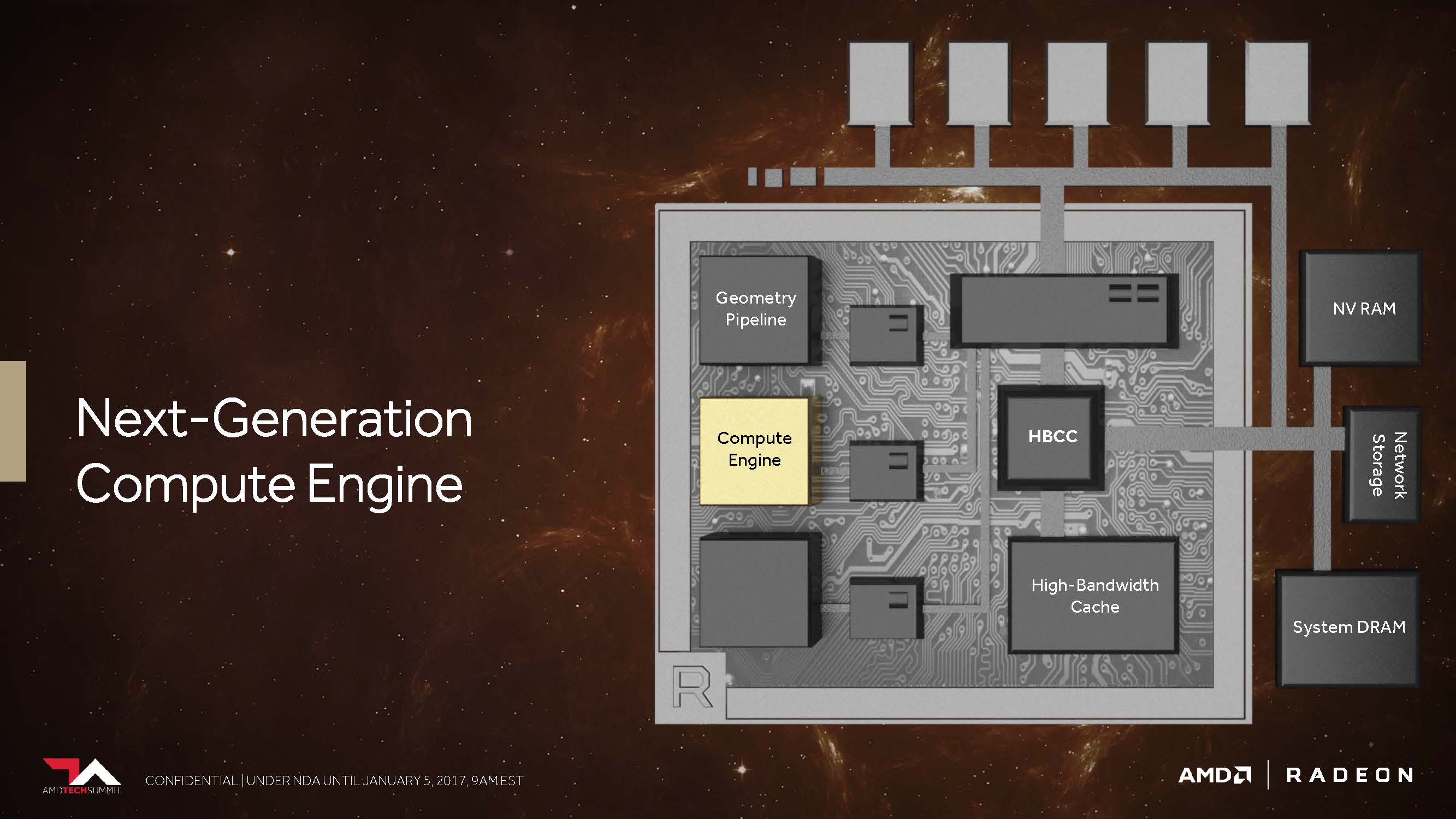
That’s the change we expect to have the largest impact on gamers as far as Vega's memory subsystem goes. However, AMD also gives the high-bandwidth cache controller (no longer just the memory controller) access to a massive 512TB virtual address space for large datasets.
When asked about how the Vega architecture's broader memory hierarchy might be utilized, AMD suggested that Vega can move memory pages in fine-grained fashion using multiple, programmable techniques. It can receive a request to bring in data and then retrieve it through a DMA transfer while the GPU switches to another thread and continues work without stalling. The controller can go get data on demand but also bring it back in predictively. Information in the HBM can be replicated in system memory like an inclusive cache, or the HBCC can maintain just one copy to save space. All of this is managed in hardware, so it’s expected to be quick and low-overhead.
Get Tom's Hardware's best news and in-depth reviews, straight to your inbox.
New Programmable Geometry Pipeline
The Hawaii GPU (Radeon R9 290X) incorporated some notable improvements over Tahiti (Radeon HD 7970), one of which was a beefier front end with four geometry engines instead of two. The more recent Fiji GPU (Radeon R9 Fury X) maintained that same four-way Shader Engine configuration. However, because it also rolled in goodness from AMD’s third-gen GCN architecture, there were some gains in tessellation throughput, as well. More recently, the Ellesmere GPU (Radeon RX 480/580) implemented a handful of techniques for again getting more from a four-engine arrangement, including a filtering algorithm/primitive discard accelerator.
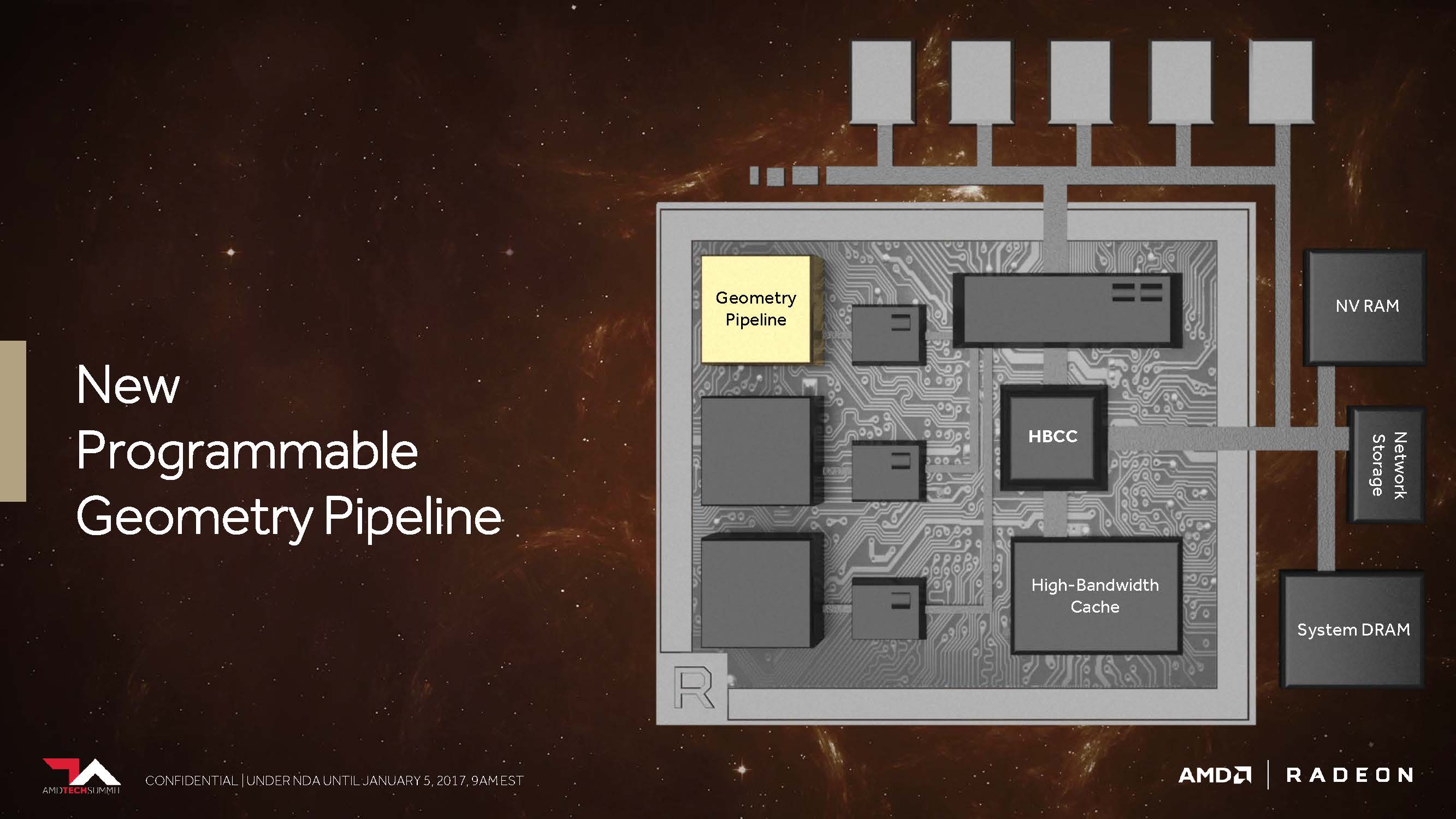
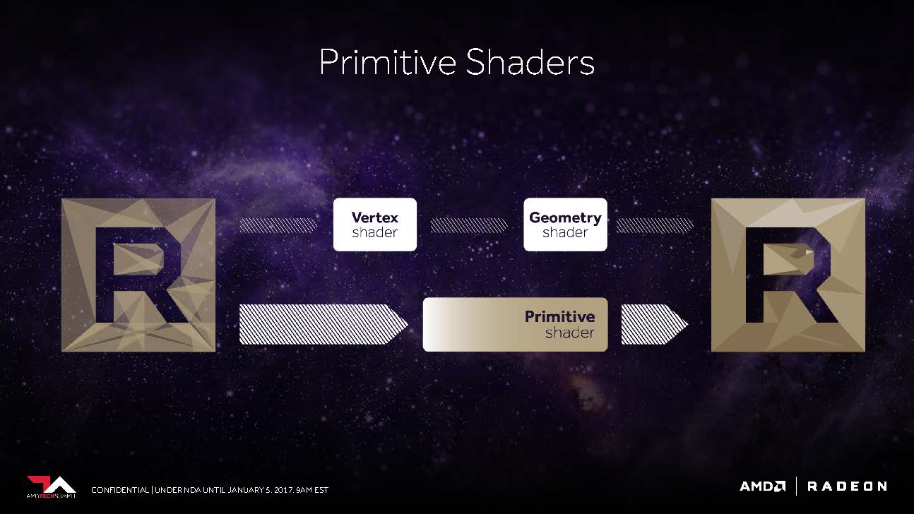
AMD promised us last year that Vega’s peak geometry throughput is 11 polygons per clock, up from the preceding generations' four, yielding up to a 2.75x boost. That specification comes from adding a new primitive shader stage to the geometry pipeline. Instead of using the fixed-function hardware, this primitive shader uses the shader array for its work.
AMD describes this as having similar access as a compute shader for processing geometry in that it’s lightweight and programmable, with the ability to discard primitives at a high rate. The primitive shader’s functionality includes a lot of what the DirectX vertex, hull, domain, and geometry shader stages can do but is more flexible about the context it carries and the order in which work is completed.
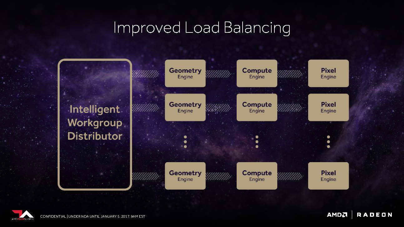
The front-end also benefits from an improved workgroup distributor, responsible for load balancing across programmable hardware. AMD says this comes from its collaboration with efficiency-sensitive console developers, and that effort is now going to benefit PC gamers, as well.
Vega’s Next-Generation Compute Unit (NCU)
Using its many Pascal-based GPUs, Nvidia is surgical about segmentation. The largest and most expensive GP100 processor offers a peak FP32 rate of 10.6 TFLOPS (if you use the peak GPU Boost frequency). A 1:2 ratio of FP64 cores yields a double-precision rate of 5.3 TFLOPS, and support for half-precision compute/storage enables up to 21.2 TFLOPS. The more consumer-oriented GP102 and GP104 processors naturally offer full-performance FP32 but deliberately handicap FP64 and FP16 rates so you can’t get away with using cheaper cards for scientific or training datasets.
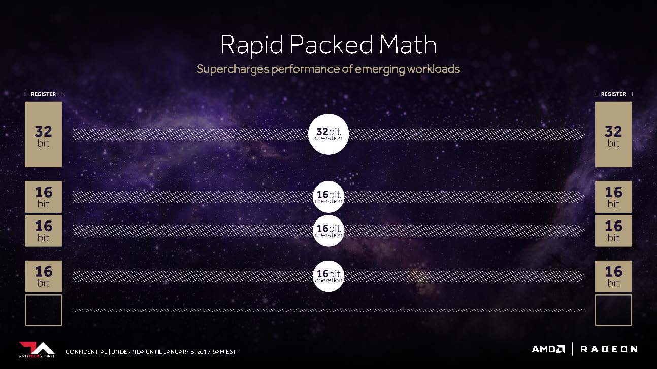
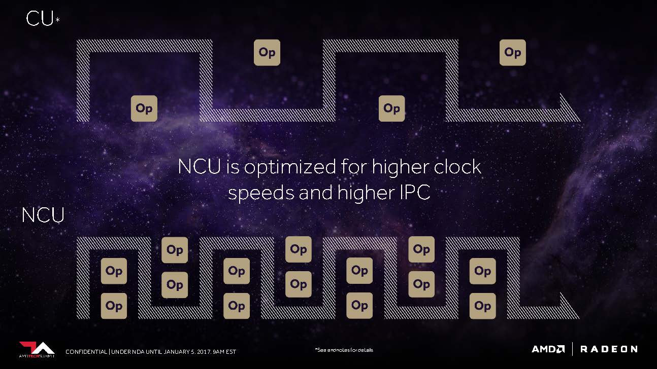
AMD, on the other hand, looks like it’s trying to give more to everyone. The Compute Unit building block, with 64 IEEE 754-2008-compliant shaders, persists, only now it’s being called an NCU, or Next-Generation Compute Unit, reflecting support for new data types. Of course, with 64 shaders and a peak of two floating-point operations/cycle, you end up with a maximum of 128 32-bit ops per clock. Using packed FP16 math, that number turns into 256 16-bit ops per clock. AMD even claimed it can do up to 512 eight-bit ops per clock. Double-precision is a different animal—AMD doesn’t seem to have a problem admitting it sets FP64 rates based on target market.
The impetus for this flexibility may have very well come from the console world. After all, we know Sony’s PlayStation 4 Pro can use half-precision to achieve up to 8.4 TFLOPS—twice its performance using 32-bit operations. Or perhaps it started with AMD’s aspirations in the machine learning space, resulting in products like the upcoming Radeon Instinct MI25 that aim to chip away at Nvidia’s market share. Either way, consoles, datacenters, and PC gamers alike stand to benefit.
AMD claimed the NCUs are optimized for higher clock rates, which isn’t particularly surprising, but it also implemented larger instruction buffers to keep the compute units busy.
Next-Generation Pixel Engine: Waiting For A Miracle
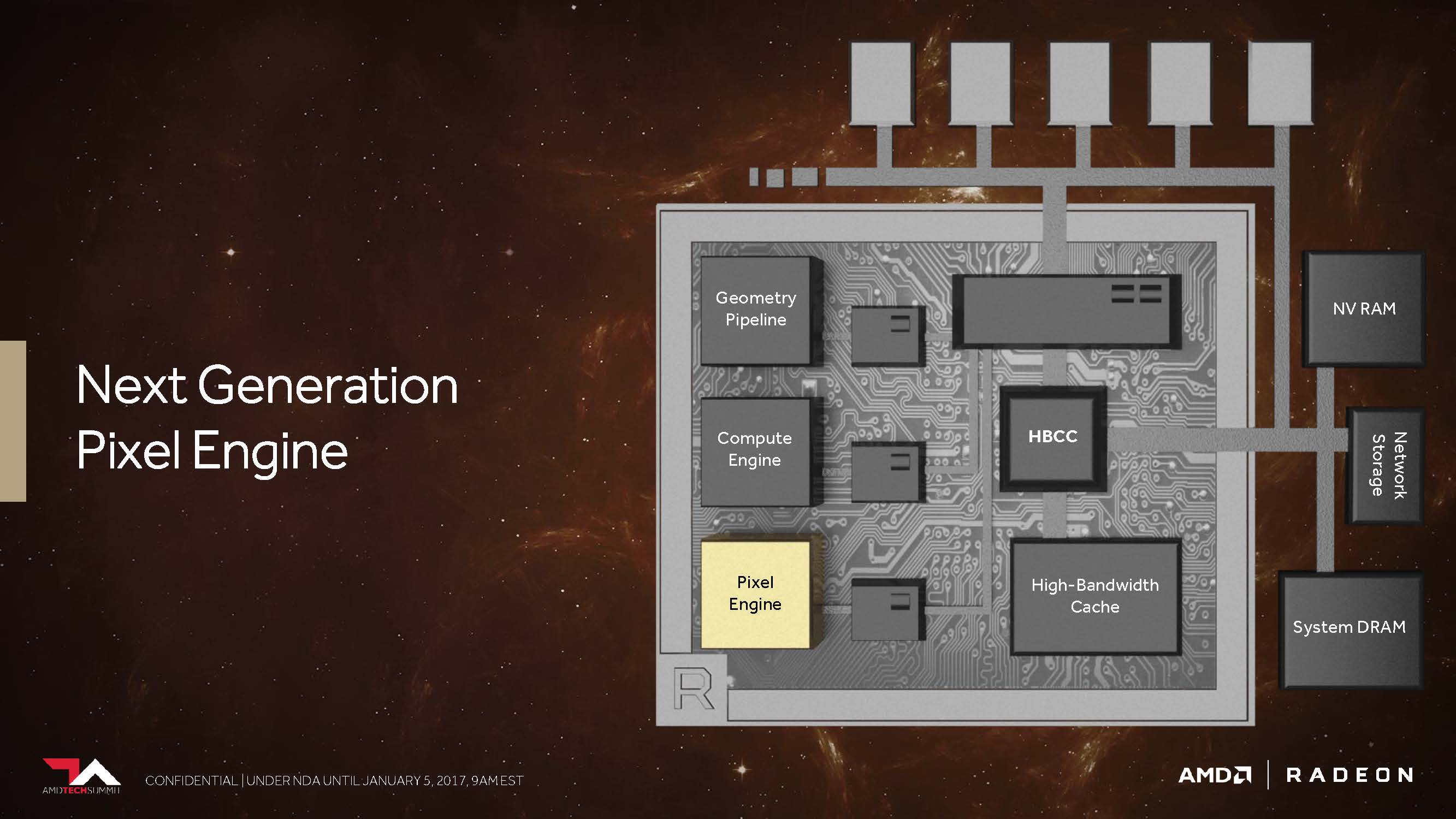
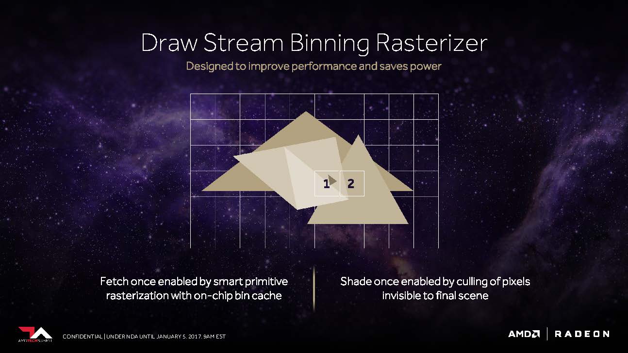
Let’s next take a look at AMD’s so-called Draw Stream Binning Rasterizer, which is supposed to be a supplement to the traditional ROP, and as such, should help improve performance while simultaneously lowering power consumption.
There’s one big question mark hanging over this feature, though. Colleagues working for several publications have run benchmarks, and none of them have recorded any significant performance improvements. The reason, we recently confirmed, is that the DSBR is currently disabled and will be made available in a future driver update.
At a high level, an on-chip bin cache allows the rasterizer to fetch data only once for overlapping primitives, and then shade pixels only once by culling pixels not visible in the final scene.
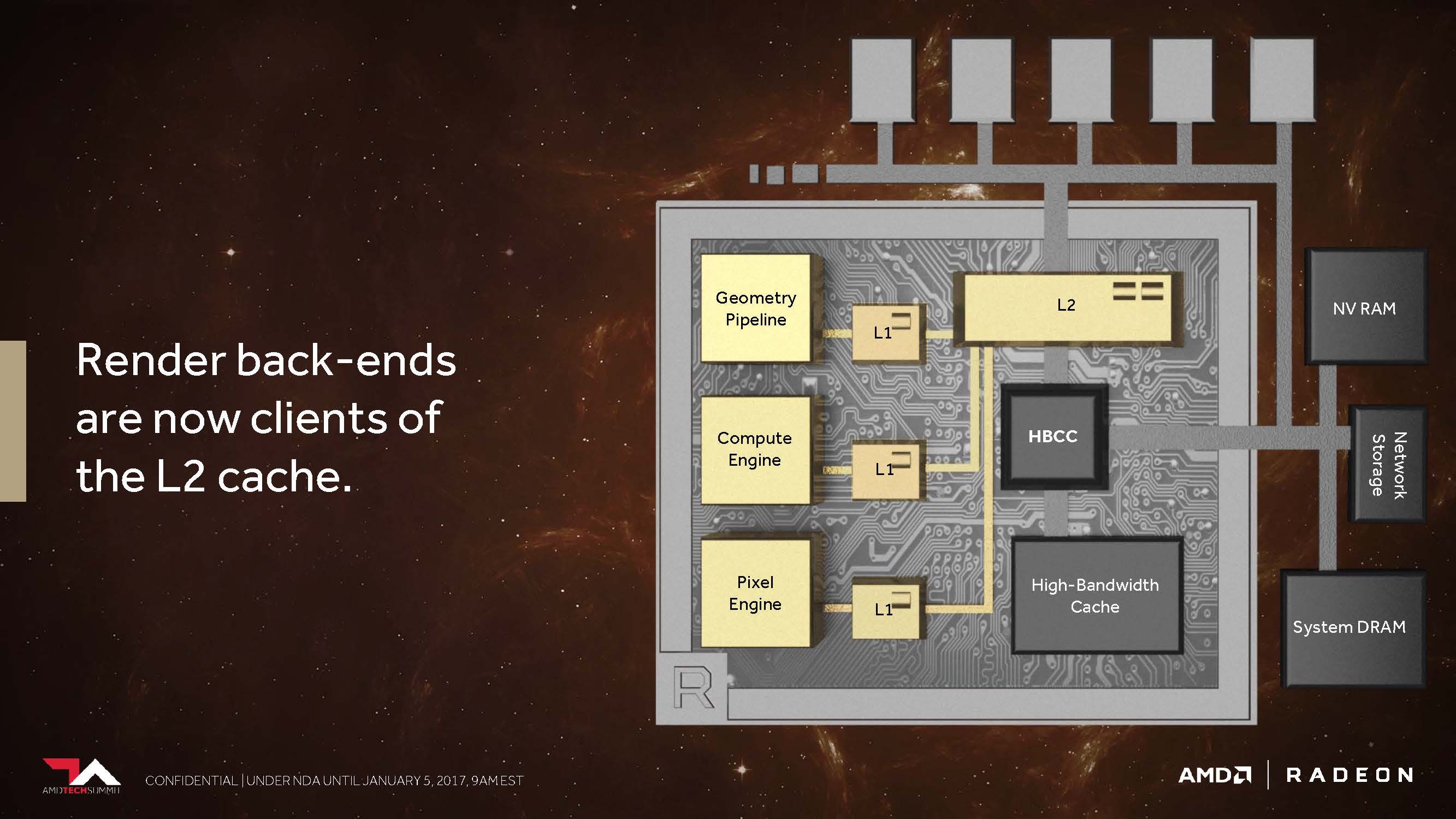
AMD fundamentally changes its cache hierarchy by making the render back-ends clients of the L2.
In architectures before Vega, AMD had non-coherent pixel and texture memory access, meaning there was no shared point for each pipeline stage to synchronize. In the example of texture baking, where a scene is rendered to a texture for reuse later and then accessed again through the shader array, data has to be pulled all the way back through off-die memory. Now, the architecture has coherent access, which AMD said particularly boosts performance in applications that use deferred shading.
MORE: Best Graphics Cards
MORE: Desktop GPU Performance Hierarchy Table
MORE: All Graphics Content
Current page: Vega Architecture & HBM2
Prev Page Meet AMD’s Radeon Vega Frontier Edition Next Page Disassembly, Cooler & Interposer
Igor Wallossek wrote a wide variety of hardware articles for Tom's Hardware, with a strong focus on technical analysis and in-depth reviews. His contributions have spanned a broad spectrum of PC components, including GPUs, CPUs, workstations, and PC builds. His insightful articles provide readers with detailed knowledge to make informed decisions in the ever-evolving tech landscape
-
Ne0Wolf7 Too bad its been so well optimized for Creo, I hate that one... Anyways, is it possible to include Autodesk Inventor in the suite? I want a card that can be used as a hybrid like this (of course I'll have to wait for it to come down in price) but its hard to decide I want something if my main software is not included in the benchmarks. Either way, I'm exited and this is a good reviewReply -
cknobman Not sure what to think here (in regards to hopes for the fx versions).Reply
I cannot expect to see a huge % boost in games just on a driver update. Maybe 10% tops?
What bothers me the most is the heat/power and throttling concerns.
I dont think those will change with a fx version of the card.
So it would appear that 80-90% of the time Vega 64 will be running closer to 1200mhz, which is a major bummer and why it wont surpass a 1080.
Almost wish there had been a review of the watercooled version as well to see if it was able to maintain higher avg mhz. -
cats_Paw Dont know much about workstation so my comment does not take that into consideration.Reply
It seems like it eats a lot of power for a very similar performance to a 1080 in gaming but at the same time its faster than Titan Xp in some workstations?
Doesn't that suggest driver/optimization issues? -
Yarvolino Ho comes that Vega and 1080Ti specs are pretty much the same, even greater numbers for Vega, and the result is that Vega is 40% slower and it drains +50% of power ?Reply
Considering Vega also costs much more, I label it as an april fool -
LORD_ORION Wow, what a horrible review.Reply
2 games, 1 resolution... and just where does this card fit in the vega lineup? You didn't even list the details of the other vega cards in a handy chart for comparison.
*starts looking for reviews on other sites* -
demonsoldier So there has been a few people tackling this and i found that lowering certain things about the card undervolting by 110mv has found to fix the clock speed issue keeping at a stable 1600 mhz with better cooling and it out performs the 1080 at that point. Can you guys do a second attempt at this with undervolts to see if that helps anything? AMD cards have been this way everytime they come out needing to have power draw issues fixed later on.Reply -
sparkyman215 Reply20013128 said:Wow, what a horrible review.
2 games, 1 resolution... and just where does this card fit in the vega lineup? You didn't even list the details of the other vega cards in a handy chart for comparison.
*starts looking for reviews on other sites*
wh-what? Toms stated like four times that this *is not a gaming card* and shouldn't be treated as one. They simply included the gaming benchmarks to be inclusive. Also, there's not really a point in showing benchmarks under 4k for such high end cards, because at that point (like 1080p) it's a CPU bottleneck - the GPU has nothing much to do. Considering listing other Vega cards, those are in a different class and not relevant, however it would be nice to have the details of the other cards, I guess. -
yeeeeman Even though AMD says with each ocassion that this graphics card is not indicative of RX Vega's performance I would say that they are trying to avoid early dissapointment. The matter of the fact is that whatever feature they have disabled right now on Vega FE, it won't bring too much performance on RX Vega. Lets face it, if they were using half of CUs on Vega FE, then I would expect huge gains from RX Vega, but as it stands, RX Vega wil be ~ GTX 1080, one year later, + 100W and hot like a stove.Reply
I really wonder how could they make a new GPU on a big better process (28nm vs 14nm) and still get more power consumption compared to Fury X. What is more surprising is that they have the same number of CUs, approx same performance with Fury X, a lot more transistors, a lot more frequency and still the improvement is minimal.
They are either hiding some huge block which doesn't do anything in graphics scenarios which consumes a lot of power just idling or they are rubbish at power optimization or maybe the HBM2 consumes a lot of power, don't know.
Everything on this card is strange, starting with performance, specs, power consumption, everything... -
Pompompaihn Seems like a very nice card if you're a home office person and need your system to do double duty. Good enough for high end gaming and comparable to expensive NVIDIA pro cards.Reply
