SK Hynix Develops HBM3 DRAMs: 24GB at 6.4 GT/s over a 1024-Bit Bus
Fast and Capacious.

SK Hynix on Wednesday introduced the industry's first HBM3 memory devices featuring a data transfer rate of 6.4 GT/s (6400 Gbps) and a bandwidth of up to 819 GB/s aimed at bandwidth-hungry applications like GPUs, CPUs, FPGAs, and AI accelerators. This new type of DRAM greatly enhances performance offered by previous generation HBM2 and HBM2E standards and add on-die error-correction code support for increased yields.
Just like previous iterations of HBM memory, HBM3 stacks multiple relatively slow DRAMs on a base die, connects them using through silicon vias (TSVs) and ties them to the host using an ultra-wide 1024-bit bus. Each HBM3stack (called KGSD — known good stacked die) supports up to 16 64-bit channels that are split into 32 pseudo channels (for finer traffic management and maximization of real-world bandwidth) with 16 to 64 banks per pseudo channel. Synopsys says that the maximum channel density is 32Gb, which means that a KGSD can pack up to 64GB of memory over a variable number of stacks.
When it comes to performance, HBM3 memory devices are not really slow, unlike early HBM and HBM2 DRAMs. Synopsys says that its HBM3 PHY supports an up to 7.2 GT/s (7200 Mbps) data transfer rate, whereas Rambus claims that its HBM3 interface supports up to 8.4 GT/s (8400 Mbps) per pin. Such rates are comparable to those of DDR5 SDRAM, though we are not sure which protocol HBM3 uses.
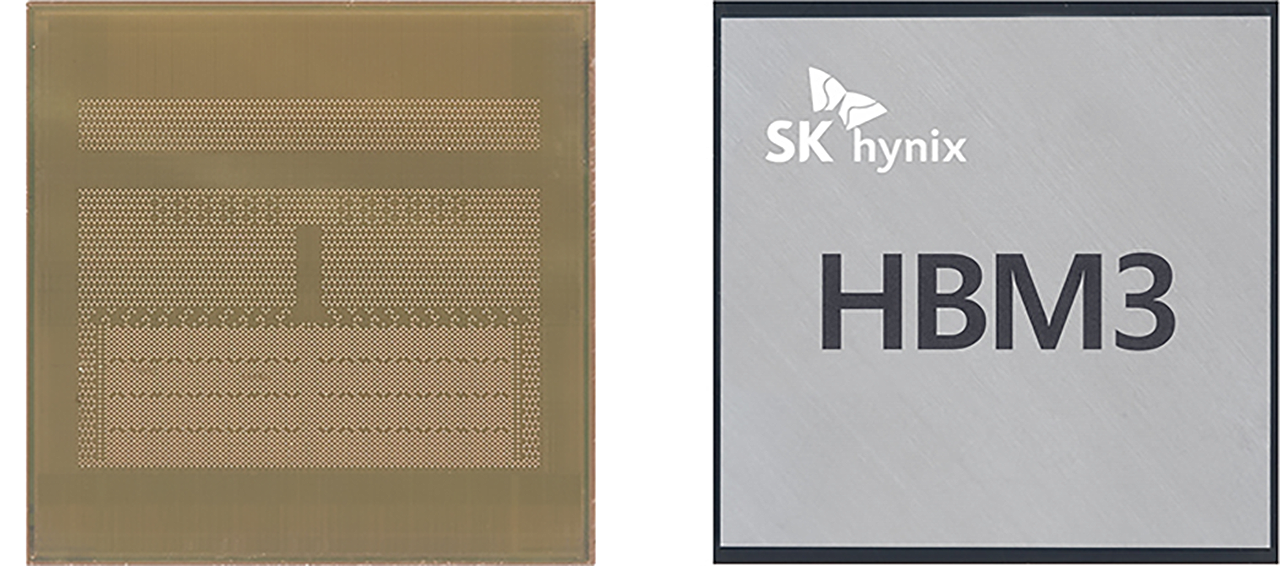
As far as SK Hynix's HBM3 family is concerned, the company plans to offer two capacity types: 16GB and 24GB. The 24GB HBM3 KGSD stacks 12 16Gb DRAMs that are 30 μm thick (each one) and interconnected using TSVs. The memory devices support a data transfer rate of 6.4 GT/s and therefore single HBM3 stack can provide a bandwidth of up to 819 GB/s. One interesting thing to note about SK Hynix's HBM3 chips is that they are square, not rectangular like HBM2 and HBM2E chips.
Typically, high-performance compute GPUs of FPGAs use four or six HBM KGSDs, so with SK Hynix's HBM3 stacks they would get a whopping 3.2 TB/s or even 4.9 TB/s of memory bandwidth.
Now that SK Hynix has finished development of its HBM3 memory products, it can start their sampling with customers eager to adopt the new type of DRAM and then mass production of appropriate KGSD devices. Unfortunately, SK Hynix does not disclose when it expects to product HBM3 DRAM stacks in high volume.
"Since its launch of the world's first HBM DRAM, SK hynix has succeeded in developing the industry’s first HBM3 after leading the HBM2E market," said Seon-yong Cha, Executive Vice President in charge of the DRAM development. "We will continue our efforts to solidify our leadership in the premium memory market and help boost the values of our customers by providing products that are in line with the ESG management standards."
Get Tom's Hardware's best news and in-depth reviews, straight to your inbox.

Anton Shilov is a contributing writer at Tom’s Hardware. Over the past couple of decades, he has covered everything from CPUs and GPUs to supercomputers and from modern process technologies and latest fab tools to high-tech industry trends.
