The Printed Circuit Board Primer
Placing The Components On The PCBs
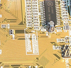
How the components are placed on the board is dependent on how they are connected. They must be placed such that the wires that link them together can be routed as efficient as possible. Efficient wiring is as short as possible and uses as few layers as possible (which also keeps the number of vias at a minimum), but we will come back to this under Routing. Below is a picture of busses routed on a PCB. It is important to place the components such that they allow such nice routing of wires.
Wires forming a Bus
Testing for routability and proper functionality when running at high speeds
At this point certain computer programs can actually check if the placement of the components will make it possible to route the wires such that the circuit will work when running at high speeds. This is referred to as proper sequencing or scheduling of the components, but we will not go into detail about this here. If the circuit appears to be malfunctioning, the components could be rearranged before the actual routing is done.
Routing The PCBs
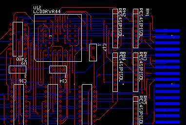
The connections in the schematic are now translated into a model of the actual conductor pattern. This process is usually automated, but manual modifications are often necessary. Below is a screenshot from the routing of a two-layer board. Red and blue lines respectively represent wires on the component and solder side of the PCB. The yellow text and rectangles are part of the silk screen that labels the locations of the components. Holes and vias are showed as dark red dots and circles. At the far right of the circuit we can see an edge-connector at the solder-side of the PCB. This final model of the PCB is often referred to as the Artwork.
Routing the PCB using CAD tools
Get Tom's Hardware's best news and in-depth reviews, straight to your inbox.
For every design a set of rules that specify minimum clearance between wires, minimum wire width and similar physical properties of the conductor pattern must be followed. These rules depend on factors like the speed of the circuit, the power of the signals that are to be transmitted, how sensitive the circuit is to leakage currents and noise, and the quality of the materials and the manufacturing equipment. The thickness of a conductor must for example be increased the more power it is required to transmit. To reduce the cost of the PCBs as few layers as possible must be used without breaking any of these rules. If more than two layers are necessary, Ground and Power planes are usually used to avoid routing wires carrying supply voltages on the signal layers, which can cause unwanted leakage currents. They also act as shields for the signal layers.
Current page: Placing The Components On The PCBs
Prev Page System Specification Next Page Test Of The Routed Circuit
