Apple's A14 SoC Under the Microscope: Die Size & Transistor Density Revealed
Examination of Apple's A14 shows a small powerhouse

ICmasters, a semiconductor reverse engineering and IP services company, has done a preliminary examination of Apple's A14 Bionic system-on-chip (SoC) using a transmission electron microscopy (TEM). An insightful report written by SemiAnalysis revealed die size and transistor density of the SoC. Such details expose the capabilities of process technologies and some aspects of the priorities of chip designers. But can a die shot of Apple's A14 give any idea about what to expect from the company's upcoming processors for notebooks and desktops?
Apple's A14 Bionic: A 88mm2 Power House
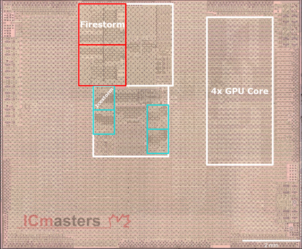
Apple's A14 Bionic SoC consists of 11.8 billion transistors and is made using TSMC's N5 (5nm) process technology. The chip packs six general-purpose processing cores consisting of two high-performance FireStorm cores and four IceStorm cores. A quad-cluster GPU, a 16-core neural engine with 11 TOPS of performance, and a variety of special-purpose accelerators complete the SoC.
The A14 Bionic processor has a die size of 88mm2, down from 98.48mm2 in the case of the A13 Bionic. The quality of the image is not exactly high, but with rough napkin math, we can gather that the dual-core FireStorm complex with a big L2 cache is around 9.1 mm2, the quad-core IceStorm complex with a small L2 cache is approximately 6.44mm2, and the GPU occupies about 11.65mm2. We know that Apple has used a unified system cache in recent years, but it is not easy to find it on the image.

The average transistor density of the A14 Bionic chip is 134.09 million transistors per mm2, up from 89.97 million transistors per mm2 in the case of the A13 Bionic, according to SemiAnalyis. Considering that semiconductor makers tend to use different methodologies when measuring transistor density, we cannot really compare TSMC's N5 to Intel's 10 nm's ~100 mega transistors per mm2, as that would be an apples-to-oranges kind of comparison. Meanwhile, Apple A14 Bionic's transistor density seems somewhat lower than TSMC's theoretical peak average transistor density promised for N5-based SoCs. This has several explanations.
Transistor density varies for different chip structures. Logic structures scale well with every new node, but SRAM, I/O, and analog parts hardy scale these days, so peak numbers advertised by foundries are highly theoretical, whereas real-world numbers are design dependent.
Designs of modern processors are extremely SRAM-intensive because SRAM is used for registers as well as caches. SRAM needs interconnects and circuitry to access it, and such interconnects do not always scale well. Given that all modern SoCs contain different types of processor cores, they also use loads of caches.
Also, parts of the chip have to operate at higher clocks (e.g., general-purpose cores). These parts can sacrifice density for performance by using high-performance cells that are usually larger. In fact, given Apple's focus on ultimate performance, its SoCs usually feature big caches (to some degree, this can be confirmed by the die shot provided by SemiAnalysys/ICmasters) and probably other performance optimizations.
Get Tom's Hardware's best news and in-depth reviews, straight to your inbox.
Indeed, A14's early performance numbers obtained in Speedometer 2.0, a browser benchmark that measures the responsiveness of Web applications by simulating rather primitive user actions, indicate that the SoC can be up to 54% faster than Intel's eight-core Core i9, which powers Apple's MacBook Pro from late 2019. Performance numbers in Speedometer 2.0 cannot give any information about performance in complex applications that are optimized for modern x86 CPUs. Still, it gives an idea about maximum theoretical performance an SoC can achieve. To some degree, this test can be considered as a drag race for modern computers.
Speculations: Can the A14 Bionic Give an Idea About Apple's SoCs for Macs?
Apple has been developing its SoCs for smartphones, tablets, smartwatches, and more recently for wearables and hearables for more than a decade now. When it needed a better-performing SoC for its iPad Air and iPad Pro tablets, it usually added CPU cores, a better GPU, more in-package memory with a wider interface, and a heat spreader for better dissipation. While it is only a speculation at this point, we can expect the company to use a similar tactic when developing its SoCs for notebooks and desktops.
Judging from dimensions of Apple's FireStorm complex and the new GPU, the company can double the number of high-performance cores and GPU clusters without significantly increasing the die size of the A14 Bionic. Of course, it will have to improve its memory subsystem (which might involve an additional 64-bit memory channel and enlarged system cache). But even with all the 'upgrades,' its SoC for PCs will have a die size similar to that of Intel's higher-end versions of Ice Lake-U CPUs that are smaller than Intel's latest Tiger Lake-U processors.
Apple has not revealed many details about its SoCs for PCs except saying that they will use the same common architecture that is used across all of its devices. Meanwhile, the company purposely called these processors 'Apple silicon' rather than something like 'A-series for Macs.'
At this point, it looks like Apple can scale its A14 Bionic design by adding CPU cores and GPU horsepower without risking making it too big. But Apple has never confirmed that it will indeed use its high-performance smartphone cores for its PC SoCs, so their usage is speculation at this point.

Anton Shilov is a contributing writer at Tom’s Hardware. Over the past couple of decades, he has covered everything from CPUs and GPUs to supercomputers and from modern process technologies and latest fab tools to high-tech industry trends.