Full Review NVIDIA's new GeForce256 'GPU'
Get Tom's Hardware's best news and in-depth reviews, straight to your inbox.
You are now subscribed
Your newsletter sign-up was successful
Introduction
The first time we heard about NVIDIA's mysterious 'NV10'-project is now more than 1.5 years ago. Still NVIDIA took time until this 'super-chip' was eventually presented to the public. It's only a month ago that 'GeForce256' was finally unveiled to us, and NVIDIA didn't lose any time to make it available to everyone soon after the announcement, although the schedule got delayed by the Taiwanese earthquake. Creative Labs were even faster than NVIDIA, they released their first boards already last week in Asia and I doubt that it will take much longer until you will be able to buy the '3D Blaster Annihilator' in the US and Europe too. I only wish that the names of those 3D-products wouldn't always have something to do with mass-murder. Since 'Napalm' I'm only waiting for a 3D-product called Hiroshima, Agent Orange or Pearl Harbor.
Anyway, to get back to the topic, what's the news about GeForce? Well, most of you will certainly have read several articles about its architecture elsewhere, and while we at Tom's Hardware don't claim to fame with regurgitating presentations or white papers, I will try and keep my summary of GeForce256 short. For those of you who require more information I deeply suggest visiting NVIDIA's website , where you can find all the white papers and presentation material you need to keep dreaming about the GeForce GPU all night long.
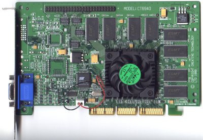
This is the GeForce256 reference board with single data rate SDRAM, actually made by Creative Labs and thus identical to '3D Blaster Annihilator'.
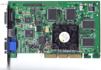
The GeForce256 reference board with DDR-SGRAM looks like this.
The Features
The most important thing about GeForce is that NVIDIA doesn't want it to be called '3D-chip' anymore. GeForce is called a 'GPU' for 'Graphics Processing Unit', and this name was chosen to give it the right honors in comparison with the all-important 'CPU'. Most of us don't realize that the complexity of today's graphics chips is at least on par with any high-end PC-processor, while the price point of 3D-chips is rather mediocre compared to a CPU. GeForce ensembles no less than 23 million transistors, which is in the same range as AMD's Athlon or Intel's upcoming Coppermine processor. Intel or AMD take more than 10 times more money for one, which makes you wonder why the 3D-chip industry is still alive. The 23 million transistors in GeForce are well spent, since it's the first 3D-chip that includes a transform and lighting ('TNL') engine. This engine is the real reason for the name 'GPU', because it adds a huge amount of computing power to GeForce, which makes it a lot more than just a chip that displays 3D-graphics.
Transform & Lighting Engine
'Transforming' is the very FP-calculation intensive task to 'transform' the 3D-scene with all its objects, called 'world-space' into the 'screen-space' that we are looking at. 'Lighting' is pretty self-explanatory, it represents on optional stage in the 3D-pipeline that calculates the lighting of objects in relation to one or several light sources. Lighting is just as transforming a pretty FP-calculation intensive task. Both tasks used to be executed by the CPU, putting rather heavy strain on it. The effect was that the 3D-chip was often in the situation that it had to wait for the CPU to deliver data (e.g. CPU-limited 3D-benchmarks) and that game developers had to restrict themselves to less detailed 3D-worlds, because heavy polygon usage would have stalled the CPU.
Get Tom's Hardware's best news and in-depth reviews, straight to your inbox.
GeForce is supposed to put an end to this dilemma, it can take the strain off the CPU, can keep the 3D-pipeline from stalling and allows game developers to use much more polygons, which automatically results in greatly increased detail. At the same time the CPU can dedicate itself to a more complex game AI or more realistic game physics. NVIDIA claims that GeForce can transform, clip and light 15-25 million triangles/s, and somewhere else I read it's at least 10 million triangles/s.
High Fill Rate
Well, even GeForce is not free from having to obey the classic demands in 3D-gaming, and one of those is asking for as much fill rate as possible. NVIDIA once claimed 500 Mpixels/s, now it's obviously shrunk to 480 Mpixels/s, but who cares, it's still way beyond the 366 Mpixels/s of the fastest current 3D-chips. I'd also like to note that I have yet to see a game that runs with a frame rate that would go hand in hand with those high fill rates. A game with dual-texturing would thus have to run at 95 fps at a resolution of 1600x1200, GeForce could do 125 fps at this resolution. I've never seen any results even close to that ... so far about those nice fill rates. GeForce achieves the 480 Mpixels/s with 4 parallel rendering pipelines and a core clock of (only?) 120 MHz.
AGP4x Fast Write
Yes! We haven't even got an AGP4x platform available on the market yet and GeForce is already faster than the rest! The 'Fast Write'-feature enables the CPU to directly write to the graphics card's frame buffer without taking a detour through system memory, and it's supposed to be up to 30% faster than 'normal' AGP4x. Let's see if Intel's 'Camino' or i820 will ever be ready and working or let's hope that 'fast write' will be supported by VIA's AGP4x 640 chipset. NVIDIA is proud to be the only 3D-chip maker that has a product supporting fast writes and NVIDIA deserves to be commended on implementing this new technology, even though I doubt that we will see much of an impact of it anytime soon. 2D as well as 3D-applications are supposed to benefit from AGP4x fast write, so you have all reason to be happy about it, regardless if you draw faster than your shadow in 3D-Westerns or type faster than your keyboard in Word.


