Sapphire Radeon RX Vega 64 Nitro+ Review
Why you can trust Tom's Hardware
Power Supply & Detailed Board Overview
Sapphire deviates significantly from AMD's reference design, and in many places, the changes make good sense. After all, the cooling is clearly optimized to lower temperatures and minimize the acoustic footprint.
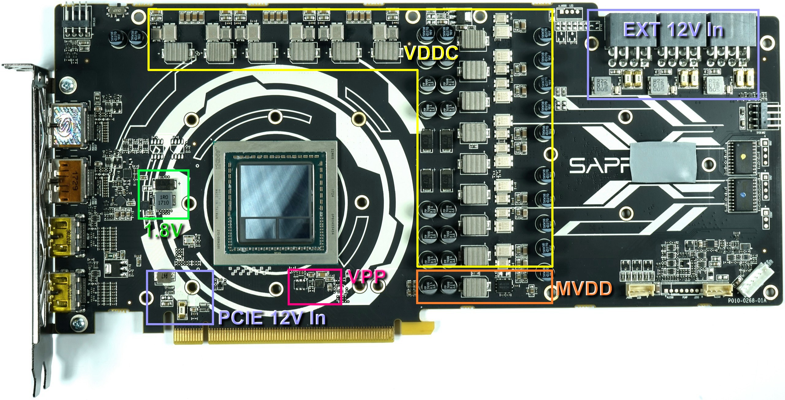
By eliminating the external memory modules, this GPU makes it easier for board manufacturers to lay out their voltage regulation circuitry. In this case, we observe a 7+1-phase implementation for the GPU and memory, along with the components needed for derivative voltages.
A trio of eight-pin auxiliary power connectors are connected via one coil each, which helps smooth out voltage peaks. No large capacitors are to be found, though.
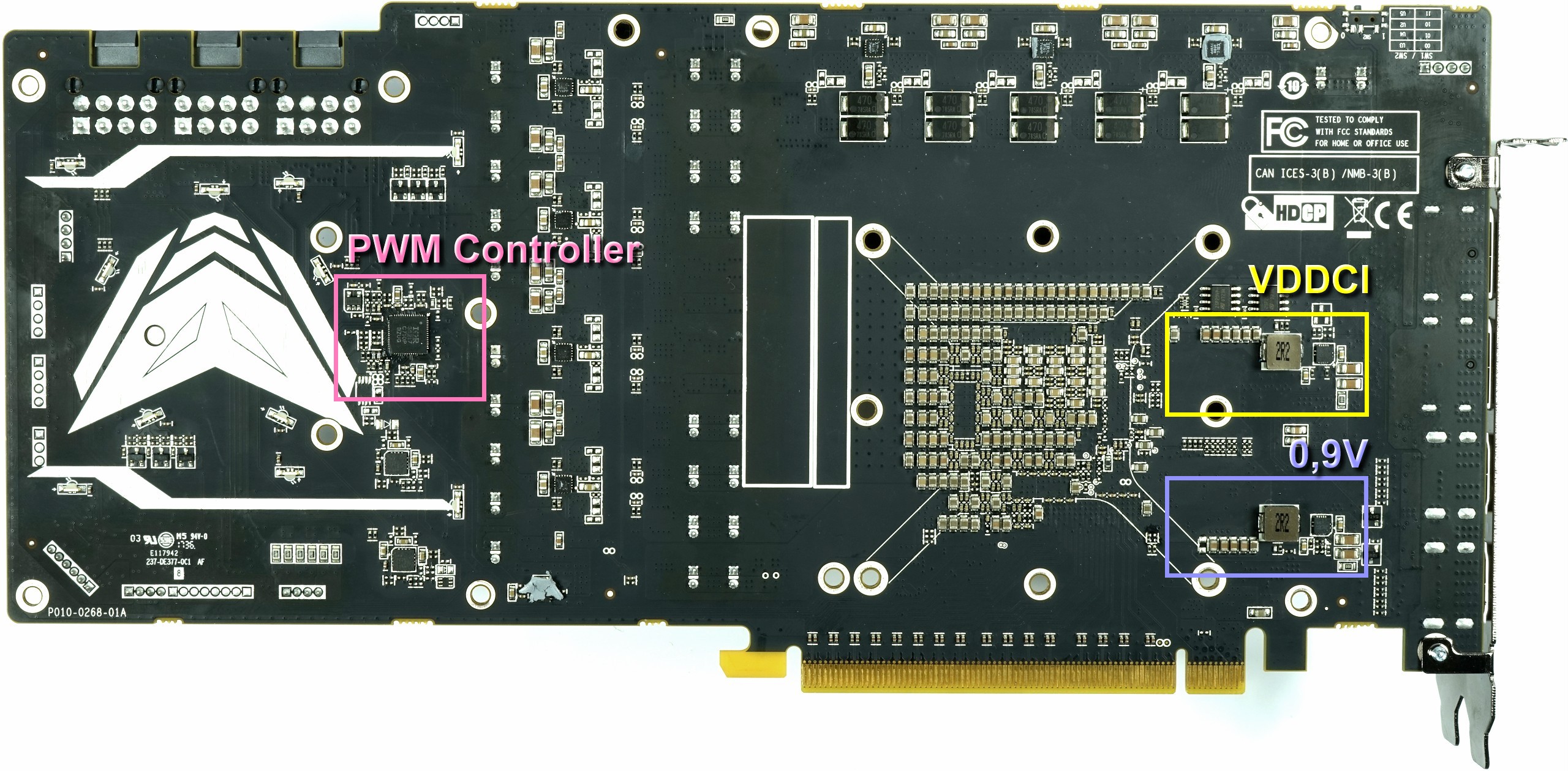
Around back, we find the PWM controller. An X6S is sufficient for the MLCC under the package, since the excellent cooler keeps temperatures low enough that Sapphire didn't need to use 125°C-class products.
Power Supply Connectors
Since it's uncommon to find a graphics card with three eight-pin PCIe connectors, we'll mention them again. Each one is protected by two 10A fuses, while the aforementioned chokes are used as filters on the input side. This helps minimize interactions between the graphics card and power supply.
Power coming from the motherboard slot also goes through a 10A fuse, as well as a common ferrite-core coil.
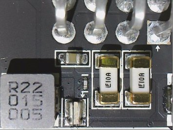
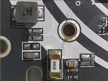
If you were looking for the shunts we often identify on GeForce cards, you can stop. There's no need for them. Vega doesn't support input-side monitoring. Instead, only the output-side current is controlled, which is easy enough to achieve with a digital PWM solution.
Get Tom's Hardware's best news and in-depth reviews, straight to your inbox.
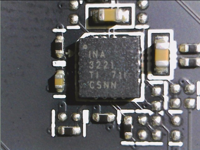
Voltage control is located on the back of the board in the form of two Texas Instruments INA3221s. This is a triple-channel monitor for the high-side and bus voltages. It supports the I2C and SMBus interfaces.
GPU Power Supply (VDDC)
International Rectifier's IR3521 sits at the center of it all (albeit on the board's back side). It functions as a dual-output digital multi-phase controller, with seven power phases for the GPU and an eighth we'll discuss next.
We count 14 voltage converter circuits instead of just seven, though. What gives? In reality, there are seven power phases that get doubled, thereby distributing load across two circuits per phase.
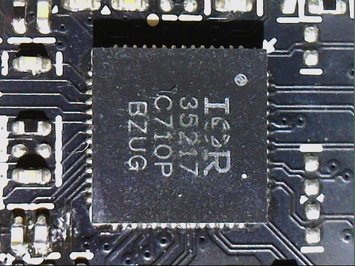
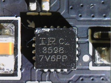
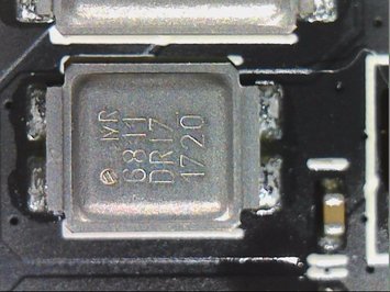
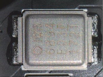
This so-called doubling is achieved through a total of seven IR3598s located on the back of the board. Voltage conversion for the 14 circuits is handled by one IRF6811 (on the high side) and one IRF6894 (on the low-side) for each circuit. Both from International Rectifier. The latter also include the necessary Schottky diode.
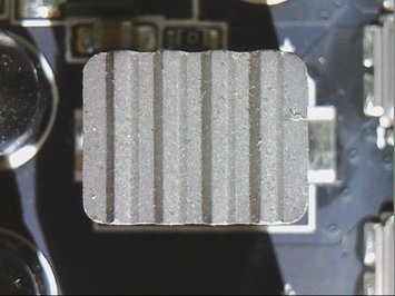
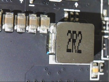
AMD likes to use "Black Diamond Chokes" for both VDDC and MVDD operation. These are essentially special encapsulated ferrite-core coils that have cooling fins on their surface. All of the other chokes, such as those for the partial voltages and input voltage filter, are just the usual encapsulated ferrite-core coils without any fancy additions.
Memory Power Supply (MVDD)
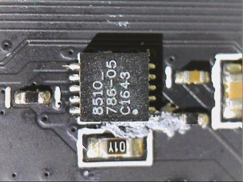
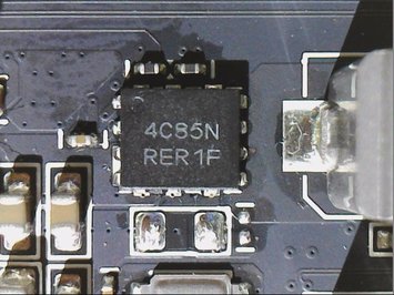
As mentioned, the memory’s single phase is also supplied by the IR35217. One phase is plenty for the HBM2 since it needs so much less power than GDDR5. The CHL815 gate driver is located on the PCB's back side, with an ON Semiconductor NTMFD4C85M used for voltage conversion. It’s a dual N-channel MOSFET able to handle the high and low sides without eating up a bunch of board space.
Other Voltage Converters
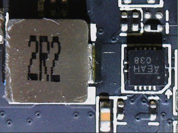
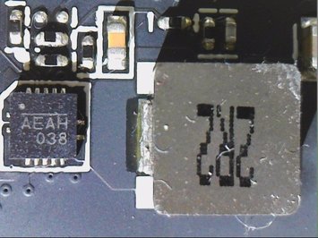
Creating the VDDCI voltage might not be particularly challenging, but it is important. It’s used for the transition between the GPU and memory signals inside the GPU. Think of it as the voltage between the memory and the GPU core on the I/O bus. There’s also a constant source of 0.9V. The two very similar voltage converters are located on the back of the board.
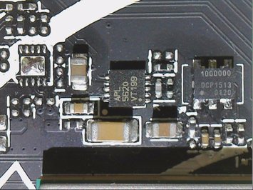
Underneath Vega 10 on the board's front side, there's an Anpec APL5620 for the VPP. It’s an ultra-low dropout part that creates a very small voltage for the phase-locked loop (PLL) section. You'll also find a 1.8V source serving TTL and GPU GPIO on the front.
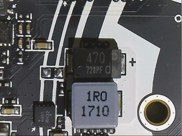
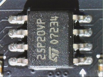
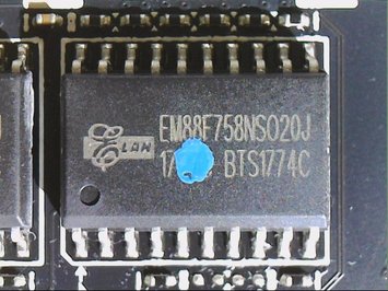
The remaining components should be pretty familiar, with the only notable exceptions being two separate ST25P20VT BIOS chips from ST Microelectronics and the pair of Elan EM88F758N programmable eight-bit controllers, which are in charge of the RGB effects and fan curve.
MORE: Best Graphics Cards
MORE: Desktop GPU Performance Hierarchy Table
MORE: All Graphics Content
Current page: Power Supply & Detailed Board Overview
Prev Page Meet Sapphire's Radeon RX Vega 64 Nitro+ Next Page Results: Ashes, BF1 & Destiny 2
Igor Wallossek wrote a wide variety of hardware articles for Tom's Hardware, with a strong focus on technical analysis and in-depth reviews. His contributions have spanned a broad spectrum of PC components, including GPUs, CPUs, workstations, and PC builds. His insightful articles provide readers with detailed knowledge to make informed decisions in the ever-evolving tech landscape
-
AgentLozen Even though Vega 64 is rough around the edges, I appreciate that you gave the Sapphire Nitro an Editor's Choice award for it's technical prowess.Reply
There is so much hardware out there with cut corners that it's nice to see something work so well. -
FormatC ReplyWhat mosfets is sapphire using for VDDC
Plase take a look at page Two. You will get the full info, pictures included. ;)
I wrote on page Two:
...This so-called doubling is achieved through a total of seven IR3598s located on the back of the board. Voltage conversion for the 14 circuits is handled by one IRF6811 (on the high side) and one IRF6894 (on the low-side) for each circuit. The latter also include the necessary Schottky diode.
-
docswag Reply20485887 said:What mosfets is sapphire using for VDDC
Plase take a look at page Two. You will get the full info, pictures included. ;)
I wrote on page Two:
...This so-called doubling is achieved through a total of seven IR3598s located on the back of the board. Voltage conversion for the 14 circuits is handled by one IRF6811 (on the high side) and one IRF6894 (on the low-side) for each circuit. The latter also include the necessary Schottky diode.
My bad, I must have skimmed over that part. Thanks! -
Cryio So once the drivers will actually apply to 3rd party OEMs as well given the reference with slower clocks is sometimes faster, will basically make Vega64 universally and sometimes significantly faster than the 1080 and guaranteed substantially faster in DX12/Vulkan games.Reply
So ... with some underclocking and undervolting, this should perform on the level of the 1080 while being more future proof. Got it.
Wonderful work AMD! Too bad miners skyrocketed the price. -
Wisecracker Thanks for the bench work. Interesting boost in minimums in some titles considering struggles with 'optimizations'Reply
What's the verdict on the previously reported 'elevation difference' between the memory stacks and processor?
-
FormatC This is randomly the molded version. That means, no difference. :)Reply
Powercolor got unmolded and the result is well-known. But I also know from others, that Sapphire is using also both packages. The 3rd package version is Vega56 only. -
FormatC It depends at your preferences, what you need in your rig. Only the price is currently a big con. Too bad.Reply
