DARPA invests $1.4 billion to build experimental Texas foundry for next-generation 3D chips — Austin plant to buck standard fab models to focus on high-mix, low-volume production
A new DARPA- and Texas-backed facility will focus on 3D heterogeneous integration, stacking, and combining multiple materials and chip types to advance U.S. capabilities in defense, AI, and HPC.

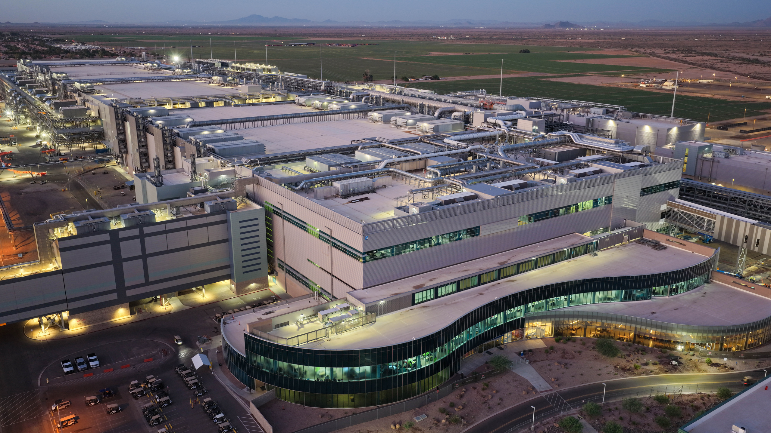
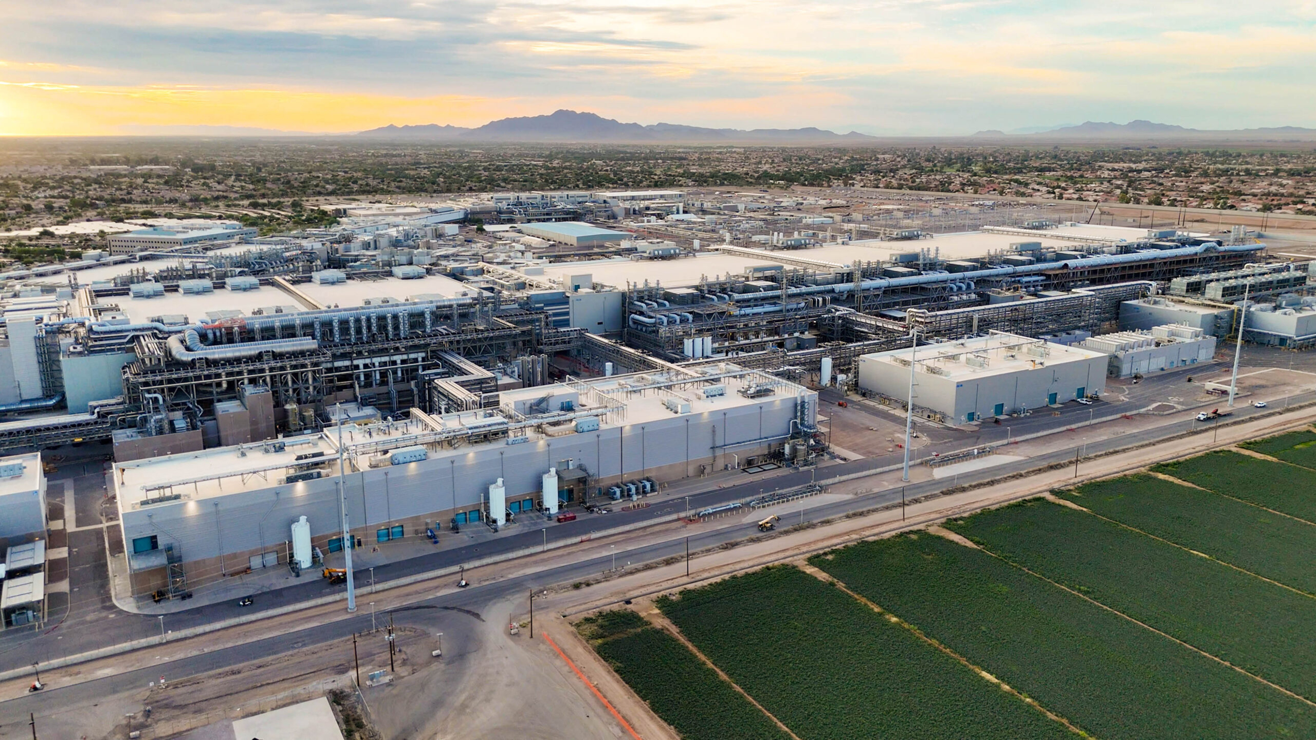
In Austin, Texas, a former 1980s chip plant is being refitted into a next-generation research foundry. Backed by $1.4 billion from the Department of Defense under DARPA’s Next-Generation Microelectronics Manufacturing (NGMM) program, the facility will concentrate on 3D heterogeneous integration (3DHI), assembling multiple chip types and materials in a single package to push beyond the limits of conventional silicon design.
The ultimate goal of this project is to close the gap between laboratory innovation and production, a persistent “lab-to-fab valley of death” that has long constrained U.S. hardware startups and defense contractors. In five years, the program is expected to transition from federal funding to a self-sustaining business serving both national security and commercial customers.
The project is a joint venture between DARPA, the state of Texas, and the University of Texas at Austin’s Texas Institute for Electronics (TIE), which will operate the fab. Housed in a refurbished 1980s-era facility, it is designed to serve as an open-access manufacturing and prototyping hub for next-generation chips that blend silicon, gallium nitride, photonics, and other advanced materials.
Article continues below“We are, frankly, a startup,” said Dwayne LaBrake, the CEO of TIE. “We have more runway than a typical startup, but we have to stand on our own,” during an interview with IEEE Spectrum.
Building a fab for ‘weird’ chips

Traditional semiconductor fabs produce monolithic silicon wafers, optimized for high-volume runs of identical designs. The Austin plant will take the opposite approach. It is being developed for high-mix, low-volume production, enabling researchers and companies to experiment with unconventional architectures and materials that mainstream foundries cannot accommodate.
DARPA program manager Michael Holmes describes 3DHI as a potential “revolution in microelectronics.” Stacking silicon on silicon, he said, can yield roughly 30-fold improvements in performance compared to 2D chips, but combining dissimilar materials could unlock up to 100-fold performance gains.
Such stacking presents formidable challenges. Dissimilar materials expand and contract differently with heat, requiring sub-micron alignment and new bonding techniques. The TIE facility is developing a process design kit (PDK) and an assembly design kit (ADK) that will codify how these materials can be combined in three dimensions, essentially creating a new design rulebook for heterogeneous packaging.
To validate its processes, NGMM is producing three demonstration systems: a phased-array radar, an infrared focal plane array, and a compact power converter. Each integrates multiple chip types, targeting critical defense applications in sensing, imaging, and power control.
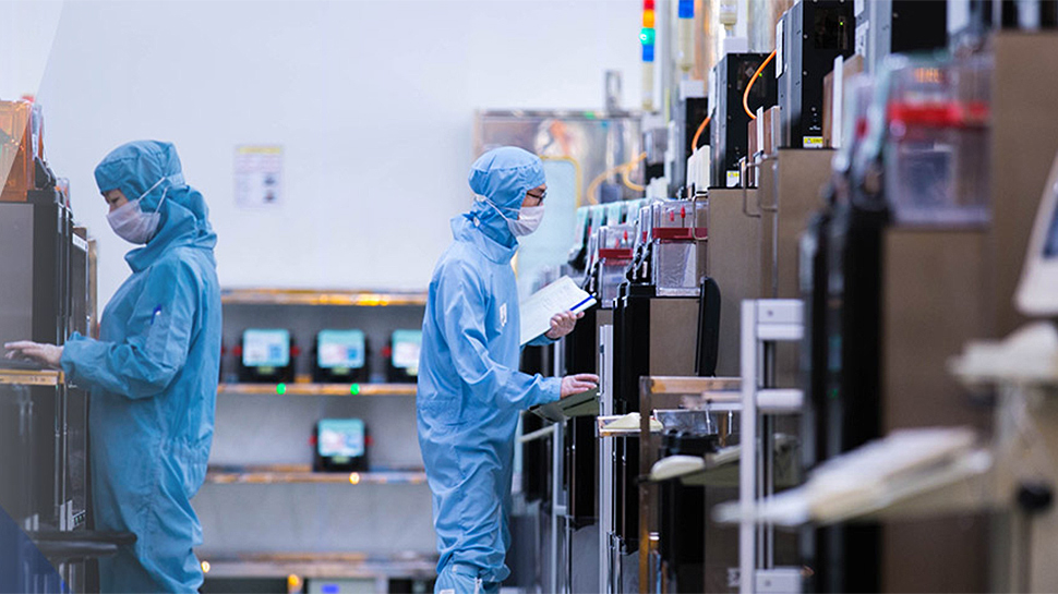
The fab’s workflow will resemble a job shop, handling diverse prototypes rather than continuous runs. To offset the inherent inefficiency of small-batch production, the team is using AI-assisted process modeling from Austin-based startup Sandbox Semiconductor, which predicts how modifying one step in the assembly line affects final yield.
Whitney Mason, director of DARPA’s Microsystems Technology Office, acknowledged that NGMM is an atypical project for the agency. “It’s not our habit to stand up facilities that do manufacturing,” she said. But with supply chain vulnerabilities exposed during recent global disruptions, DARPA sees domestic advanced packaging as a strategic necessity.
3D stacking meets chiplets
DARPA’s experiment comes as the semiconductor industry itself pivots toward multi-chip packaging. Apple, Intel, AMD, Nvidia, and TSMC all rely on some form of advanced integration to extend performance gains, now that transistor scaling alone can no longer keep pace with demand.
Intel has invested heavily in this direction through its IDM 2.0 strategy, pairing new fabrication nodes with technologies like Foveros and EMIB, which connect multiple dies within one package. In 2024, Intel opened its $3.5 billion advanced packaging hub in New Mexico, capable of bonding chiplets made on different process nodes. The company’s packaging expertise has already landed it a $5 billion collaboration with Nvidia, which will use Intel’s Foveros technology to combine GPU and CPU chiplets on a single package.

AMD and TSMC, meanwhile, have taken chiplet integration mainstream. AMD’s MI300A accelerator integrates thirteen chiplets — CPUs, GPUs, I/O, and stacked HBM3 memory — inside one module. TSMC provides the 2.5D and 3D packaging infrastructure that underpins AMD, Apple, and Nvidia’s flagship products through its CoWoS and SoIC platforms. Apple’s M1 Ultra uses TSMC CoWoS to fuse two M1 Max chips at a combined 2.5 TB/s inter-chip bandwidth.
DARPA’s NGMM differs in both scope and purpose. Commercial packaging focuses on connecting silicon dies for higher performance or memory bandwidth. The Austin fab targets heterogeneous integration across materials and device classes, assembling sensors, power amplifiers, and logic circuits that would never share a wafer in traditional production. It also aims to provide open access, allowing small companies and researchers to experiment without the massive entry costs of a private fab.
The initiative dovetails with a wider federal strategy. While NGMM is funded by the Department of Defense, it complements the CHIPS and Science Act’s National Advanced Packaging Manufacturing Program, an effort to expand domestic R&D infrastructure for chip assembly and test. Together with Intel’s expansions and Amkor’s planned Arizona facility — which will package Apple’s U.S.-made chips from TSMC’s Phoenix fab — NGMM represents a three-pronged attempt to rebuild a complete onshore supply chain.
Stacking the future
High-performance computing and AI chips are already constrained by thermal density and memory bandwidth, areas where 3DHI could offer breakthroughs. Integrating logic and memory vertically could shorten signal paths and reduce power, while new materials such as microfluidic cooling films or on-package photonics could allow stacked layers to operate without overheating.
For AI systems, that means faster interconnects and lower latency between compute units, which is an urgent need as model sizes climb into the trillions of parameters. For defense, it promises more compact, power-efficient electronics for radar, imaging, and communications, all designed and built domestically.
The Austin fab also serves a longer-term industrial goal of proving that a low-volume, high-complexity foundry can be financially sustainable. Once DARPA’s five-year funding runway ends, TIE plans to operate as an independent commercial entity supported by government contracts and specialty manufacturing orders. The viability of that model will depend on whether its unique capabilities can attract a steady pipeline of customers in the aerospace, computing, and energy sectors.
Ultimately, NGMM reflects a growing consensus that semiconductor innovation is now concerned with what’s above the wafer, not within it. The Austin facility’s success will depend heavily on execution, because building reproducible processes for 3DHI is far more complex than packaging homogeneous silicon dies — and creating a business from that foundation is harder still. Yet if it delivers on even part of its promise, NGMM could establish a new center of gravity for U.S. semiconductor research and manufacturing complements, rather than competes with, traditional fabs.
Follow Tom's Hardware on Google News, or add us as a preferred source, to get our latest news, analysis, & reviews in your feeds.


Luke James is a freelance writer and journalist. Although his background is in legal, he has a personal interest in all things tech, especially hardware and microelectronics, and anything regulatory.
