Intel Document Confirms New LGA1700 Socket For Alder Lake Processors

It feels like a bad nightmare. Intel's LGA1200 socket for Comet Lake processors isn't even a year old yet, and there are already talks of a new socket for next year's 10nm processor.
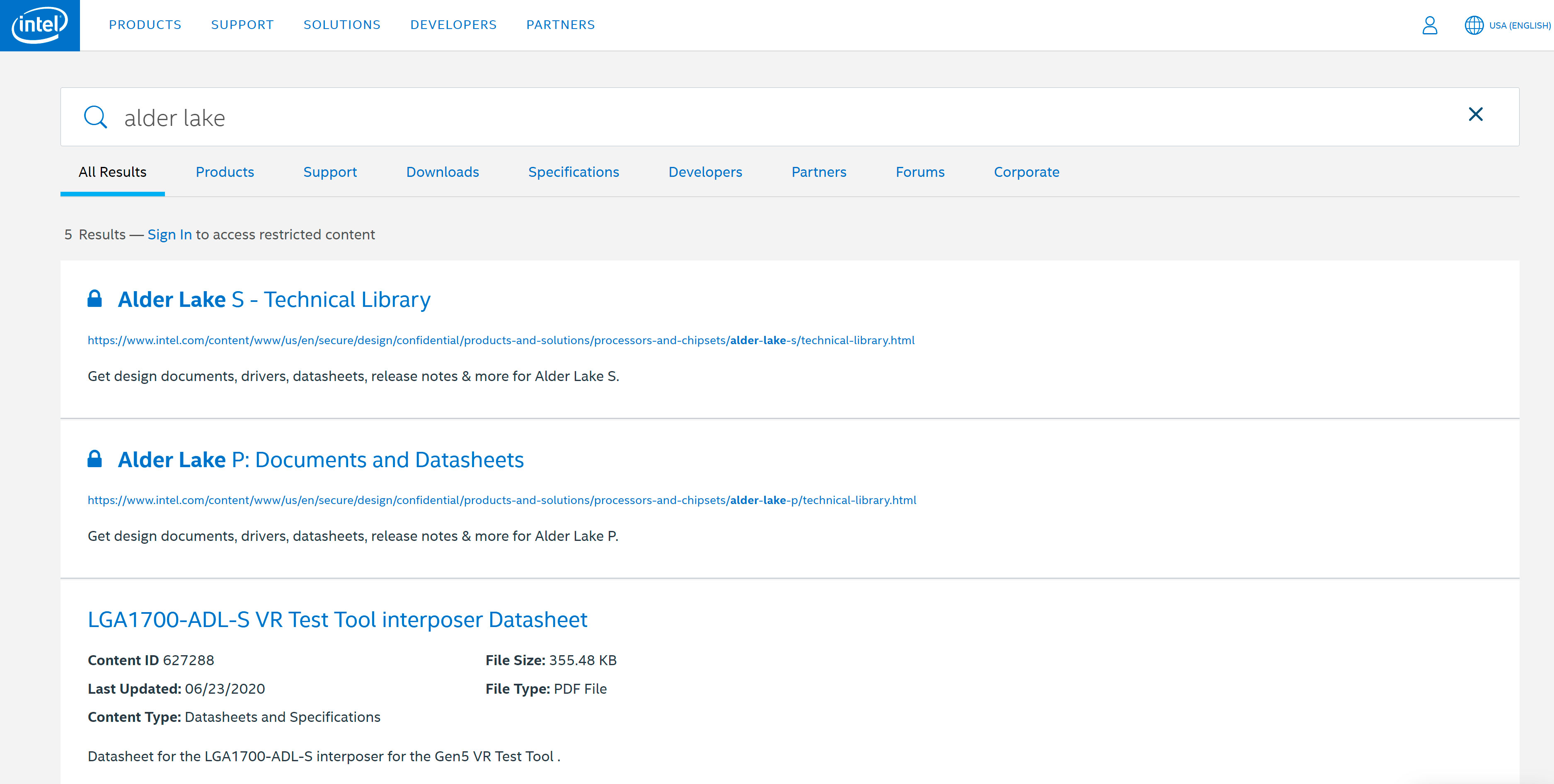
The latest Intel document (via @momomo_us) seemingly confirms that 12th Generation Alder Lake processors willprobably land with the LGA1700 socket. Alder Lake-S refers to the desktop processors, while the Alder Lake-P is a mystery for now.
Intel's nomenclature for its sockets has remained unchanged over the years. As the name implies, the LGA1700 socket will likely come with 500 more pins, which represent a 41.7% pin increase over the existing LGA1200 socket. It'll be interesting to see how Intel distribute the additional pins, and whether LGA1700 socket proves to be wider or longer than the LGA1200 socket.
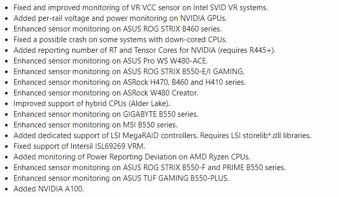
Normally, the excess pins are there to deliver more power to the processor, support new features or expand I/O capabilities. In Alder Lake's case, it could be all of the aforementioned. Intel's recent Lakefield processors brought a hybrid design that combines powerful cores with energy-efficient cores, similar to Arm's big.LITTLE microarchitecture. The current buzz around town is that Alder Lake could bring this same concept to the desktop, and that's seemingly confirmed by a recent HWinfo update that lists Alder Lake as a "hybrid CPU," which is Intel's nomenclature for the big.LITTLE-esq implementation in Lakefield.
Lakefield blends one big core with four smaller cores into a five-core package. Alder Lake, on the other hand, could break cover with a 16-core design that merges eight big cores with eight small cores. Lakefield employs Sunny Cove and Tremont for the high-performance and low-powered cores, respectively.

Alder Lake might utilize a combination of Golden Cove and Gracemont cores, the first being the successor to Willow Cove and the latter for Tremont. However, there isn't any evidence that remotely backs up this hypothesis. The rumored thermal limit for Alder Lake is 125W and if so, it would be on the same grounds as Comet Lake.
There are a lot more hearsay on Alder Lake, and for now, we should take them with a pinch of salt. In terms of support, Alder Lake allegedly welcomes the PCIe 4.0 interface and DDR5 memory. Being a 10nm part, Alder Lake likely leverages Intel's Xe graphics, but it's unclear which generation of the iGPU will be featured inside the chip.
Get Tom's Hardware's best news and in-depth reviews, straight to your inbox.

Zhiye Liu is a news editor, memory reviewer, and SSD tester at Tom’s Hardware. Although he loves everything that’s hardware, he has a soft spot for CPUs, GPUs, and RAM.
-
1_rick I read somewhere that the new chip will be rectangular--whereas the substrate is somehting like 37x37mm now, the LGA1700 will be 47x37mm, if I remember correctly.Reply -
Kamen Rider Blade There's no way in hell the new Socket will be the same dimensions as LGA 1200.Reply
It has to increase in size given the number of new pins.
That means you'll probably need a new spec for coolers to mount to along with more surface area for the heat spreader.
That means all old LGA 1200/115x coolers will be obsolete. -
bit_user ReplyIt feels like a bad nightmare. Intel's LGA1200 socket for Comet Lake processors isn't even a year old yet, and there are already talks of a new socket for next year's 10nm processor.
A year? Didn't it just launch a couple months ago?
Still, there's nothing new. After Comet Lake comes Rocket Lake. And that's two generations, which means it's time for a new desktop socket. That's how Intel rolls.
The only exception to that was Haswell, which launched with a new socket that only lasted 1 generation, since the Broadwell desktop CPUs were pretty much all cancelled.
Intel even went so far as to introduce some trivial incompatibilities between Kaby Lake and Coffee Lake. Not to say that the new socket delivered no benefits, but a few boards have been made supporting all 4 generations - from Skylake to Coffee Lake-R, showing just how minor the differences must really be. Why they went ahead with it is anyone's guess - no doubt power-delivery was one reason, but AMD seems to have addressed such matters without changing their socket. So, perhaps it was motivated by wanting to keep commitments to their board partners and force a few extra sales?
As for the function of the 500 additional pins, I'm going to speculate that it could have something to do with Thunderbolt / DP 2.0 / USB 4. -
TCA_ChinChin If the top end desktop chips also have the big little configuration, I'm going to be a little confused. It makes sense for lower power applications that need efficiency such as laptops, but if you're going to be selling to the diy builder space, most people are not going to want those little cores. Whats the point, especially if you need specific scheduling to make the most out of the big.little config?Reply -
bit_user Reply
I had a similar reaction, when I first read about it. However, in a previous thread, someone pointed out that it lets them advertise the chip as 16 cores and should give them a not-insignificant multi-threaded performance boost over having just the 8 "big" cores.TCA_ChinChin said:If the top end desktop chips also have the big little configuration, I'm going to be a little confused. It makes sense for lower power applications that need efficiency such as laptops,
If we consider that each "little" core is about 60% as fast a "big" core, yet uses about 40% of the area and maybe only 30% of the power, then it's both a more power- and area- efficient way to scale performance for highly-threaded workloads. Plus, they get better idle power numbers, by running backgound tasks on the "little" cores.
And all of the necessary software support should already be in place for Lakefield.
When you look at it like that, it really seems pretty obvious. Of course, I pulled the numbers out of the air, but I believe they're in the general ballpark, based on the slides they published (and other available info) on Lakefield. -
InvalidError Reply
The clearance area on the motherboard is more than large enough to accommodate a larger socket as long as whatever HSF you may want to reuse does not have stuff hanging below it that would interfere. The IHS may be bigger but the only thing that matters is whether the main heat-generating dies are covered.Kamen Rider Blade said:That means you'll probably need a new spec for coolers to mount to along with more surface area for the heat spreader.
As for what the 500 pins might be for, my guess is Intel has brought the chipset on-package, so ~300 of those pins are HSIO lanes with their associated power/ground pins and the bulk of the remaining 200 pins are for chipset power. -
TCA_ChinChin Reply
I hope you're right, cause if software support isn't impeccable, its gonna suffer. If all the cores also have hyperthreading (im don't remember if they do or not or if Intel has actually said anything about that) it'll make things a lot more bearable.bit_user said:I had a similar reaction, when I first read about it. However, in a previous thread, someone pointed out that it lets them advertise the chip as 16 cores and should give them a not-insignificant multi-threaded performance boost over having just the 8 "big" cores.
If we consider that each "little" core is about 60% as fast a "big" core, yet uses about 40% of the area and maybe only 30% of the power, then it's both a more power- and area- efficient way to scale performance for highly-threaded workloads. Plus, they get better idle power numbers, by running backgound tasks on the "little" cores.
And all of the necessary software support should already be in place for Lakefield.
When you look at it like that, it really seems pretty obvious. Of course, I pulled the numbers out of the air, but I believe they're in the general ballpark, based on the slides they published (and other available info) on Lakefield. -
InvalidError Reply
Which is pretty much what GPUs do. Each individual core/shader may be only 1/10th as fast but there are nearly 1000X as many so you get ~50X as much performance per watt and ~20X the performance per area.bit_user said:If we consider that each "little" core is about 60% as fast a "big" core, yet uses about 40% of the area and maybe only 30% of the power, then it's both a more power- and area- efficient way to scale performance for highly-threaded workloads. -
bit_user Reply
According to this:TCA_ChinChin said:I hope you're right, cause if software support isn't impeccable, its gonna suffer. If all the cores also have hyperthreading (im don't remember if they do or not or if Intel has actually said anything about that) it'll make things a lot more bearable.
https://en.wikichip.org/wiki/intel/microarchitectures/tremont
...there's no indication of HT. I think only the first-gen Atom cores had Hyperthreading. Tremont is now about the 5th major revision of the uArch, not counting node-shrinks and lumping Goldmont/Goldmont+ together.
BTW, I noticed the article mentioned Gracemont - the one after Tremont - but Wikichip has basically nothing on it.
https://en.wikichip.org/wiki/intel/microarchitectures/gracemont -
bit_user Reply
It's true, but in this case (pretty much all big+little setups, AFAIK), the cores have the same architecture state. That means the OS can trivially & seamlessly move threads back-and-forth between the big & little cores, which is not something you can do between CPU & GPU cores.InvalidError said:Which is pretty much what GPUs do. Each individual core/shader may be only 1/10th as fast but there are nearly 1000X as many so you get ~50X as much performance per watt and ~20X the performance per area.
For software to support "heterogeneous processing" of a common task between CPUs + GPUs, the code has to be separately compiled for each, and software has to explicitly manage sharing of the workload between them. It doesn't come for "free", like in the big+little scenario. I'm sure you know this, but I'm just explaining for the benefit of others.
