Silverstone SST-EP03 Tear-Down
Get Tom's Hardware's best news and in-depth reviews, straight to your inbox.
You are now subscribed
Your newsletter sign-up was successful
The Great And Powerful Fluxie!
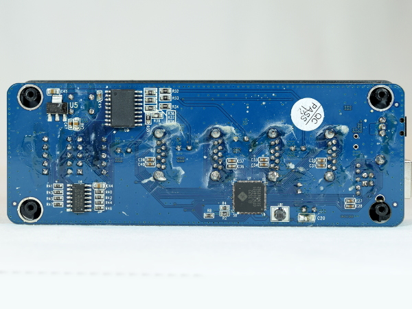
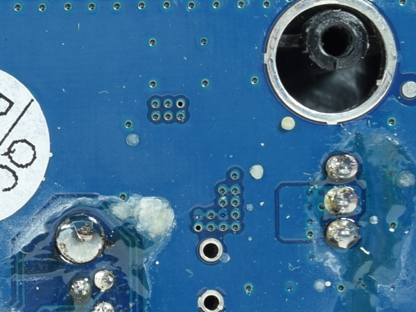
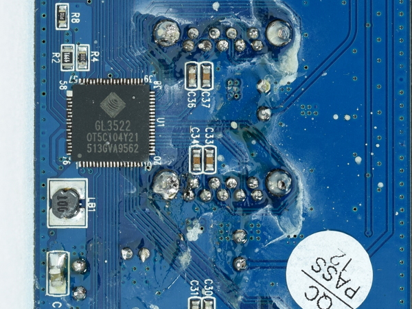
If I had to hand out a title for “fluxiest-looking board” to a manufacturer, I believe Tripp-Lite would have to turn it over to SilverStone. Thankfully, electrons don’t care how crusty a PCB looks. Whatever that high-tack flux is, it is solid at room temperature, softens at about 150°C, and remains greasy beyond 200°C. I can see why manufacturing left it there.
From left to right, we have the display multiplexer and LED current-limiting resistor array for the meter IC, two extra ceramic bypass capacitors for each port’s power, and the hub IC itself.
MORE: Best Deals
MORE: Hot Bargains @PurchDeals
Solder Blobs
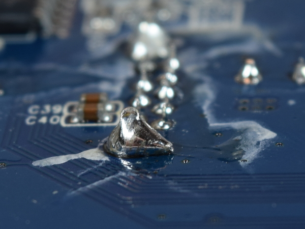
If the generous amount of flux around through-hole components wasn’t enough of a clue, the inconsistent through-hole soldering quality gives away that through-hole soldering was done by hand. This is especially evident on the connector shield solder tabs. That's a large blob with a long tail. To be fair, this was by far the worst solder joint I could find.
Most manufacturers that do double-sided load boards put all of their BGAs, QFNs, and fine pitch components on the top, glue the remaining surface-mount components with exposed pads to the bottom, and wave-solder everything to eliminate hand-soldering and achieve repeatable quality.
MORE: Best Power Supplies
Get Tom's Hardware's best news and in-depth reviews, straight to your inbox.
MORE:10 Inexpensive Automotive USB Adapters Tested
Clean-Up
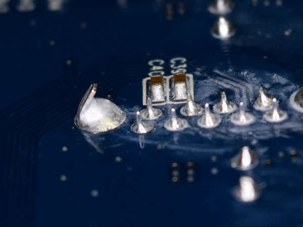
Seeing such a large blob nagged me, so I decided to put my knife soldering tip on and clean it up, along with the other shield tabs. All I had to do was shove its edge down the inside of the tab and pull it away to remove the excess solder.
The white residue around the pins is the aftermath of my first flux cleaning attempts: mixing isopropanol with the flux caused it to turn from hard and light brown to waxy, tacky, and white.
MORE: Best PC Builds
MORE: Best Cases
Missed Me?
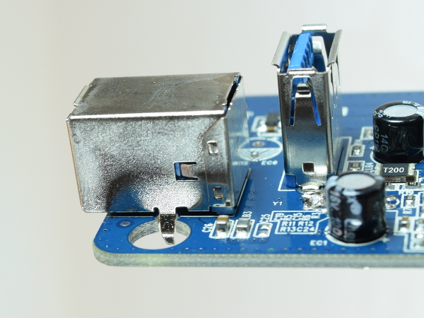
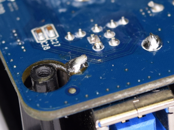
Can you spot the problem in this picture? I initially missed it while examining the top side of the PCB. One of the Type B connector shield’s tabs was left unsoldered. You can clearly see the B-shield’s tab going down the hole in the bottom-left corner. Why is that? The B-connector’s footprint is too close to the mechanical hole, so the two holes end up intersecting. You are seeing the tab because a quarter of its hole overlaps the mechanical hole.
Time for one more soldering touch-up.
MORE: Best Deals
MORE: Hot Bargains @PurchDeals
Touch-Up
Since the shield tabs provide the connector with some additional mechanical strength, I bent the tab over the thin sliver of a solder pad on the remainder of its hole, fluxed that up, then applied heat until solder attached to the pad. Whoever did the manual soldering on this board should have handled the job; there clearly aren’t any mechanical clearance issues associated with it.
The partial pad issue could have been avoided by simply moving the USB connector two or three millimeters closer to the DC-in jack (they are six millimeters apart) and re-arranging the Q1 circuit accordingly.
MORE: Best Power Supplies
MORE:10 Inexpensive Automotive USB Adapters Tested
Vias To Nowhere
When I first looked at Q1’s circuitry and noticed the via clusters around it, I figured that the FET must be expected to occasionally get hot enough to require thermal vias. When I flipped the board around, I expected to see small copper pours covering those via clusters and spreading heat around more effectively
After scratching my head for a while, I realized that I hadn’t seen traces for 5V leave the Q1/DC-in area on either side of the board. Despite the top and bottom looking sparse enough for this to look like it could be a two-layer PCB job, it must have at least one internal layer for a 5V plane and that’s where Q1’s heat would go.
That said, I’d still like to see a copper pour to join clusters of same-rail thermal vias.
MORE: Best PC Builds
MORE: Best Cases
Secret Sauce
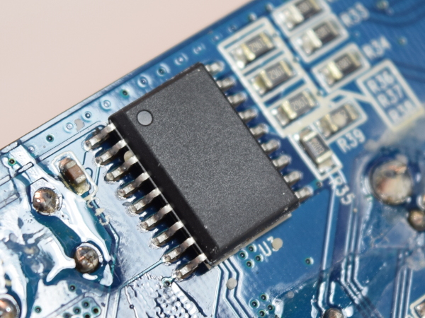
What chip does the EP03 use to provide voltage and current measurements? A completely unmarked SO-18 black box. Why use sand, laser, lacquer, grinding, or pay for custom markings to obfuscate information when you can simply order components unmarked? Since this mystery chip uses a 74HC164 serial-to-parallel converter to drive the LEDs, it must be a micro-controller with an 8:1 analog input multiplexer for its ADC.
I do not remember seeing any logic chip from a major brand with VDD on pin #1 and VSS on pin #18 or whatever number the first pin on either side of a dual row package may be, so I’ll guess that this must be a generic Chinese micro-controller.
MORE: Best Deals
MORE: Hot Bargains @PurchDeals
Braiiins!
The Genesys Logic GL3522 looks lonely on the bottom side since nearly all of its support components are located on the top layer, clearing the way to fan out five sets of six USB signals: D+/- for legacy USB, RX+/- and TX+/- for USB 3.0, one set for each of the four downstream port, and a fifth set for the upstream port.
To give the chip some immunity against noise that could make its way from attached devices into the hub’s 5V supply, its internal linear regulators are fed via a 100µH inductor labeled LB1, which rests on over-sized pads with C20 and EC1 providing supply bypass immediately upstream from it.
If C20 (bottom-left corner) looks odd to you, that’s because you are seeing a 0603-size part on a 0805-size footprint.
MORE: Best Power Supplies
MORE:10 Inexpensive Automotive USB Adapters Tested
Inside The GL3522
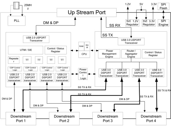
What do you find inside of a USB 3.0 hub chip? To start, two fundamentally independent hubs: a USB 2.0 repeater to handle the D+/- signals for backward compatibility with pre-3.0 devices, and a separate USB 3.0 router to handle the SuperSpeed (SS) RX/TX pairs. The two halves share a single CPU, which takes care of little more than hub enumeration and link power state management.
Since SuperSpeed has its own enumeration process over the SS links, it should be technically possible to operate the 2.0 and 3.0 hubs independently to provide four 2.0-only and four 3.0-only downstream ports. I would gladly sacrifice one-port-fits-all backward compatibility for additional usable ports on a hub.
MORE: Best PC Builds
MORE: Best Cases
Quick AC Adapter Assessment
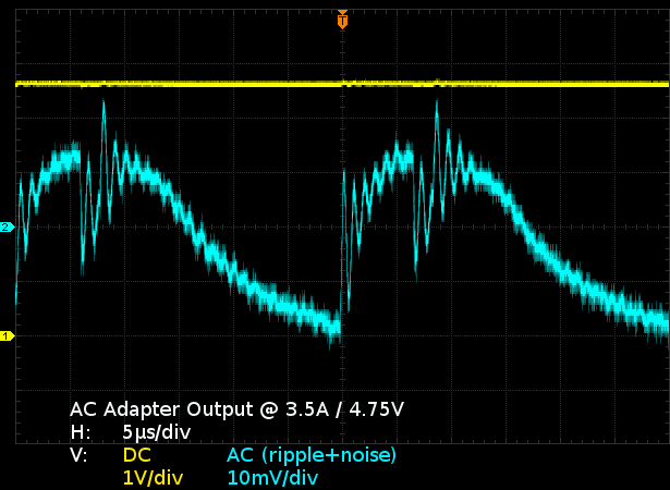
How much power does the Fullpower adapter from Shenzhen use, and how efficient is it? With no load attached, its standby power draw is a respectable 0.22W, easily beating the 0.3W requirement of its level V efficiency class. Under 1A of output load, its output voltage is 5.04V with 6.41W of input power, yielding an efficiency of 78.6%, again beating level V’s 68.2% requirement at 5W and even level VI’s 73.7%. At 3.5A, the output drops to 4.75V while input power is 19.77W for an efficiency of 84.1%, still beating VI’s 82% requirement by two whole points. Regardless of load, ripple remains between 40 and 50mVPP.
Apart from the 5% voltage drop under full-rated load, this appears to be a decent little adapter. At a glance, the only reason it did not earn a VI efficiency mark is that VI demands 0.1W or lower idle power.
MORE: Best Deals
MORE: Hot Bargains @PurchDeals
-
Daniel Sauvageau Many people say that reviewers get cherry-picked samples. As my contact at Silverstone told me when I sent him a copy of my tear-down as a heads-up for what was coming, reviewers get whatever inventory is in the warehouse like everybody else and I doubt anybody will dispute that here.Reply -
itsnotmeitsyou This was awesome. Thanks for this kind of content TH. Makes this feel like a real technically oriented website instead of just tech gossip. Kinda felt like that was where things were headed for a while.Reply -
jtd871 Good on SilverStone for asking for your unvarnished criticism. But it's disappointing that SS's own QA/QC doesn't pick up these issues.Reply -
Daniel Sauvageau Reply
Most of these were more 'quibbles' than serious issues though: as long as the flux is non-corrosive at room temperature, there is nothing technically wrong with leaving the finished PCB drowned in it. Solder blobs may not be pretty but as long as they don't touch anything they shouldn't, there is nothing wrong with those either. Ripples and noise on VBus may not be pretty but section 11.4.4.2 of the USB 3.1 spec (VBus) does not have a noise or ripple specification. Anything from 4.45V to 5.25V appears to be fair game.18896400 said:Good on SilverStone for asking for your unvarnished criticism. But it's disappointing that SS's own QA/QC doesn't pick up these issues.
The only real issue I have with it is the mechanical/shield hole on the upstream port since leaving one tab loose means more stress on the data pins when the cable gets (dis)connected or tugged. SilverStone told me one tab is enough, but I don't have to like it.
