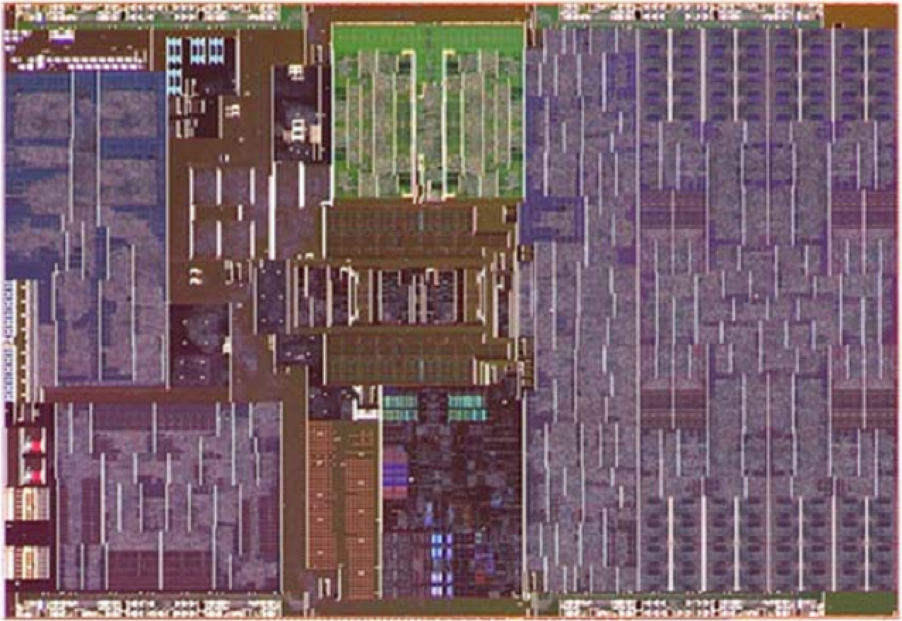
Intel Lakefield Die Shot Shows 82mm² Chip
Lakefield die shot shows one Sunny Cove and four Tremont cores.
A die shot has appeared online of Lakefield, Intel’s first 3D stacked chip that comes courtesy of Foveros technology. It has a die area of 82mm².

The die shot comes from Imgur and was found by an AnandTech Forums member. According to the image information, the Lakefield die is 82mm², just as large as the dual-core 14nm Broadwell-Y. The green area in the middle would be the Tremont cluster, measuring 5.1mm², while the dark area below it at the bottom center would be the Sunny Cove core. The GPU at the right, which includes media and display engines, consumes about 40% of the die.
When Intel detailed Lakefield, Foveros and its hybrid architecture last year, it only said that the total package size was 12mm x 12mm. This small package size is due to the 3D stacking using Intel's Foveros technology: within the package is a base die on 22FFL connected to the 10nm compute die via the Foveros active interposer technology. The compute die contains one Sunny Cove core and four Atom Tremont corex. Above the chip, there is also PoP (package-on-package) DRAM.
We posted a hands-on with the first Lakefield device at CES, the Lenovo X1 Fold.
Get Tom's Hardware's best news and in-depth reviews, straight to your inbox.